rfbrw said:
Rather than go around in circles one can read the relevant datasheets, implement burst or stopped clock operation and study the results. Till then all one can do is speculate.
As I don't have the hardware to do that, I will not experiment.
I think I rode the relevant datasheet. I understand something, you understand another thing...
But It doesn't matter, I'm on the AD1865 now (yes, it's not up to date, but I had the circuits), and I can't have two works on the same time, my working table is too small 😀
We will not stay on this problem all the year long.
And as I said at the beginning, It's easy to reclock the two signals if we doubt.
Have a good day
Philippe
philbyx said:
And as I said at the beginning, It's easy to reclock the two signals if we doubt.
Have a good day
Philippe
this is true, though I prefer to directly clock the most important clock pin of a DAC directly, with the least amouint of gates in-between
I did this yesterday in a cheap CD player, implementing one of my clocks. You could hear the typical improvement but after I also directly clocked pin 1 of the TDA1543, thing realy started to sing.....
cheers
Guido Tent said:
Very interesting guys !
Another method could be to deliberately add jitter on BCK and WCK and see what yields the highest distortions.....
cheers
In my setup BCK does no more than load the serial register, so jitter on it does not matter.
rfbrw said:
In my setup BCK does no more than load the serial register, so jitter on it does not matter.
except for the internal crosstalk.....(but this effect depends on DAC type and is for those who want to squeeze out the last part of performance)
cheers
I just finished my DF1704/PCM1704 dac.
The BCK of the dac is clocked directly off one of Guido's oscillators. The other signals come from the DF1704. I'd thought that such a setup would eliminate the need for lownoise/high quality psu for the DF.
However, when I use a lownoise reg for the DF, instead of a 7805, the sound is much nicer (less digital and more details).
This experience would support the claim that WCK jitter does indeed affect the performance of the PCM1704. From the datasheet this is not apparent (Like a lot of things. Reading the datasheet gives the feeling that there must be additional information available somewhere. Surely this can't be everything BB wants to share with us?).
It is mentioned that it is possible to reclock the WCK. How can this be done. Is there a simple solution for this (such as dividing the BCK by 64) that is actually low on jitter?
ABO said:I just finished my DF1704/PCM1704 dac.
The BCK of the dac is clocked directly off one of Guido's oscillators. The other signals come from the DF1704. I'd thought that such a setup would eliminate the need for lownoise/high quality psu for the DF.
However, when I use a lownoise reg for the DF, instead of a 7805, the sound is much nicer (less digital and more details).
This experience would support the claim that WCK jitter does indeed affect the performance of the PCM1704. From the datasheet this is not apparent (Like a lot of things. Reading the datasheet gives the feeling that there must be additional information available somewhere. Surely this can't be everything BB wants to share with us?).
It is mentioned that it is possible to reclock the WCK. How can this be done. Is there a simple solution for this (such as dividing the BCK by 64) that is actually low on jitter?
congratulations (the DF is a nightmare to solder)
Do you use I2S and if so do you feed the drive with the same clock ?
Reclocking WCK could be done with a D type flipflop, I assume. I wouldn't divide it that much down, seems more complex than the Dff
cheers
ABO said:I just finished my DF1704/PCM1704 dac.
It is mentioned that it is possible to reclock the WCK. How can this be done. Is there a simple solution for this (such as dividing the BCK by 64) that is actually low on jitter?
You will find on this link my setup where I reclock Wclk on ad1865 with a guido oscillator mounted on a daughter board of the Dac board.
I think that this is the simpliest way to do (dual ff 74act74).
http://www.diyaudio.com/forums/showthread.php?postid=554767#post554767
In my setup, I send the clock to the cdrom driver also.
You have somme photos later in the topic.
The dac works since a week, and the sound seems to be very good.
(my old drive is a panasonic twenty years old !).
Philippe
Guido Tent said:
except for the internal crosstalk.....(but this effect depends on DAC type and is for those who want to squeeze out the last part of performance)
cheers
What internal crosstalk? Data is static before conversion and BCLK does not start up till well after conversion has taken place.
rfbrw said:
What internal crosstalk? Data is static before conversion and BCLK does not start up till well after conversion has taken place.
But the conversion clock still may be affected by the signals entering the chip.....
Guido Tent said:
But the conversion clock still may be affected by the signals entering the chip.....
At the time of conversion there are NO signals entering the chip.
rfbrw said:
At the time of conversion there are NO signals entering the chip.
Hi,
At the moment of conversion, there are no signals changing from their digital state, but at steady state (logic 0 or 1) the noise (e.g. groundbounce) on these lines may affect the conversion clock.....
Proper reclocking takes away the noise
enjoy the weekend
Guido Tent said:
Hi,
At the moment of conversion, there are no signals changing from their digital state, but at steady state (logic 0 or 1) the noise (e.g. groundbounce) on these lines may affect the conversion clock.....
Proper reclocking takes away the noise
enjoy the weekend
You cannot reclock static volatile data any more than you can reclock the pits on a CD disc . The data is static. It is not moving. It is not changing value. Groundbounce is not an issue as the data has had more than enough time to settle, BCLK is tied low and WCLK is high waiting to go low. By all means reclock WCLK but thats as far as it goes. At this point beyond a clean power supply and seeking to create an electronically benign enviroment for the chip there is nothing to be done.
rfbrw said:
What internal crosstalk? Data is static before conversion and BCLK does not start up till well after conversion has taken place.
In the setup that started this whole thread an FPGA is clocked async to the BCLK. BCLK goes straigt between CD drive and DAC board with a minimum of gates inbetween. The FPGA polls BCLK to know when to update SDATA and WCLK.
According to figure 1 on page 7 of the 1704 datasheet, SDATA is read at the positive edge of BCLK. My Verilog code detects a positive edge a little while after it happens, and then updates SDATA and WCLK in time before the next positive edge.
So SDATA should be static at the positive edge of BCLK. It certainly looks like the DAC output is also updated on the positive edge of BCLK. Therefore, the only sources of crosstalk I can see at this critical time are 1 - Ringing on digital signals, and 2 - late/early SDATA which would probably be audible if it occured on this edge.
Greetings,
Børge
Guido Tent said:
Hi,
At the moment of conversion, there are no signals changing from their digital state, but at steady state (logic 0 or 1) the noise (e.g. groundbounce) on these lines may affect the conversion clock.....
Proper reclocking takes away the noise
enjoy the weekend
I don't know about TI/BB, but in the chips I have been laying out, the first thing a digital input signal encounters after having crossed the bond wire and pad protection resistors/diodes, is a couple of inverters that buffer it on its way inward on the chip. A common (digital) supply voltage is usually employed for all these buffers.
Here's my hypothesis:
If an input signal is static at 0 or 1, the current consumed by its pad buffer is very small. It is only with severe noise that a pad buffers start drawing enough current to upset its supply voltage enough that the other pad buffer (the one handling BCLK) inserts considerable jitter. Or maybe ground bounce will inject enough current through the series protection resistors that there will indeed be an upset internal power supply? Because then things would improve with reclockers close to the chip driven off clean supplies.
Greetings,
Børge
Hi
From a new member
Re the 1704
I thought that the 1704 did some internal conversion from 2s
complement to some other coding scheme which seems to take
two clock cycles hence it is the fall of the second bit clock when the DA conversion is done.
Geoff
From a new member
Re the 1704
I thought that the 1704 did some internal conversion from 2s
complement to some other coding scheme which seems to take
two clock cycles hence it is the fall of the second bit clock when the DA conversion is done.
Geoff
uhmmm.... my two cents...
Hi, all...
Let´s think on jitter at all: time domain errors in digital signal that leads to a wrong conversion value (in time, obviously). Please correct me if I'm wrong...
So, if PCM1704 as former 1702 also, depends on the " rising edge of bclk " signal to change the voltage value of the output, as stated in datasheet, jitter at bclk should affect the time it occurs. So... it will lead to the mentioned time domain error.
My reading of datasheet : the combination of Low state of the WDCK AND the numbered RISING edge of BCLK lead to change the output value, NOT the conversion, but that change SHOULD occur at precise time to minimise jitter effect. So, BCLK should be precisein time, although not constant.
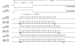
We can observe PMD100 datasheet when it does operate stopped clock output, the first rising edge of bclk is precise relative to XTI signal (type of MCK ).
IMHO, to have a very precise MCK, SCK, XTI or anything like those and carefull PCB layout, is MUCH more important than introduce gates to reclock sck and wdck signals.
Sorry for long post. 😀
😎
Regards to all
Euclides.
Hi, all...
Let´s think on jitter at all: time domain errors in digital signal that leads to a wrong conversion value (in time, obviously). Please correct me if I'm wrong...
So, if PCM1704 as former 1702 also, depends on the " rising edge of bclk " signal to change the voltage value of the output, as stated in datasheet, jitter at bclk should affect the time it occurs. So... it will lead to the mentioned time domain error.
My reading of datasheet : the combination of Low state of the WDCK AND the numbered RISING edge of BCLK lead to change the output value, NOT the conversion, but that change SHOULD occur at precise time to minimise jitter effect. So, BCLK should be precisein time, although not constant.
We can observe PMD100 datasheet when it does operate stopped clock output, the first rising edge of bclk is precise relative to XTI signal (type of MCK ).
IMHO, to have a very precise MCK, SCK, XTI or anything like those and carefull PCB layout, is MUCH more important than introduce gates to reclock sck and wdck signals.
Sorry for long post. 😀
😎
Regards to all
Euclides.

- Status
- Not open for further replies.
- Home
- Source & Line
- Digital Source
- pcm1704: Jitter on WCLK