The datasheet for the Burr-Brown pcm1704 says that
"The serial-to-parallel data transfer to the DAC occurs on the falling edge of WCLK. The change in the output of the DAC occurs at the rising edge of the 2nd BCLK after the falling edge of WCLK".
Does that mean I can have a jittery (as in generated by async or poorly PLL'ed FPGA) WCLK as long as BCLK is nice? I respect all setup and hold time specs when I interface the converters.
Greetings,
Børge
The change in the output of the DAC occurs at the rising edge of the 2nd BCLK after the falling edge of WCLK
Nothing to do with the falling edge of wclk. The important is bclk only.
wclk can be jittery, it's a rising edge of bclk which have te be at time without jitter.
Some Dac (ad1865 for example) need a perfect wclk, because it is the falling edge of wclk which transfers the datas from the shift register to the parallel register of the dac.
But in your case, best effort on bclk.
Philippe
børge said:
The datasheet for the Burr-Brown pcm1704 says that
"The serial-to-parallel data transfer to the DAC occurs on the falling edge of WCLK. The change in the output of the DAC occurs at the rising edge of the 2nd BCLK after the falling edge of WCLK".
Does that mean I can have a jittery (as in generated by async or poorly PLL'ed FPGA) WCLK as long as BCLK is nice? I respect all setup and hold time specs when I interface the converters.
Greetings,
Børge
Ummm, it seems philbyx's datasheet for the PCM1704 differs from mine. In the datasheet I have, WCLK determines the transfer of data into the parallel register and thus conversion i.e. WCLK reflects the sample rate the dac is running at. Furthermore, according to my datasheet, BCLK for 24bit/44K1 data can vary between 8MHz and 11MHz and can be stopped altogether such that it is not running when conversion takes place. Now, I don't have much time for all this clock fetishism but I would focus my efforts on WCLK.
Why argue about datasheets? Just go to www.ti.com and
download the latest and most up-to-date-est.
It is clearly defined on page 7 as Borge quoted.
download the latest and most up-to-date-est.
It is clearly defined on page 7 as Borge quoted.
BrianL said:Why argue about datasheets? Just go to www.ti.com and
download the latest and most up-to-date-est.
It is clearly defined on page 7 as Borge quoted.
It isn't about the datasheet. It is about whether WCLK is more important than BCLK. As WCLK triggers conversion and BCLK need not be present at conversion, I maintain that WCLK is more important than BCLK.
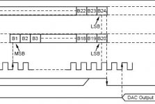
Hello Rfbrw
Two minutes ago, I went to TI focus.
I put the timing diagram below in my post.
It's quite obvious that Bclk will synchronize the analog part of the Dac.
The Dac output will be changed by Bclk.
Wclk has a only internal effect (loading of intermediate registers I think) and the Jitter on it has no effect on analog output rythme.
Philippe
Attachments
philbyx said:Hello Rfbrw
Two minutes ago, I went to TI focus.
I put the timing diagram below in my post.
It's quite obvious that Bclk will synchronize the analog part of the Dac.
The Dac output will be changed by Bclk.
Wclk has a only internal effect (loading of intermediate registers I think) and the Jitter on it has no effect on analog output rythme.
Philippe
Hi
As I read it, this is correct, I rephrase the datasheet
" The change in the output of the DAC occurs at the rising edge of the 2nd BCLK after the falling edge of WCLK "
It is also my experience when applying the 1704, bck is very sensitive.
However, internal crosstalk may affect the bck jitter, so I suggest to reclock all digital signals entering the 1704. At least in the DCA we designed using the 63 it helped.
best regards
Hi Guido
I don't understand what you mean .
Philippe
At least in the DCA we designed using the 63 it helped.
I don't understand what you mean .
Philippe
I have worked with the PCM1702 before. That one latched on the 4th BCLK after WCLK. (I know because I had a sample and hold circuit on the same board. Don't ask why...)
The PCM63 was the predecessor of the PCM1702 if I got this right.
In my setup, there is an FPGA which uses its own async clock. I pick the 11MHz from the cd player, buffer it there with a 74HC04, and feed it directly to BCLK on the DAC. The FPGA polls BCLK so that it knows what do do with with SDATA and WCLK.
The reason I didn't reclock SDATA and WCLK was that I wanted to avoid excess circuits and noise sources at the critical 11MHz. Rather, I thought the async FPGA clock would spread any noise coupled from those signals over frequencies that are not harmonic products of my sample rate.
Statistically, this should give the arrival time of a WCLK or SDATA edge a flat distribution which is 10ns long. Relative to a BCLK edge, that is. (Because of the async 100MHz clock of the FPGA.) Comments?
I know the '04 buffering of the CD player clock is not the best idea ever. Next addition is to put a nice clock on the analog board, close to the DACs, buffer it and run the CD player transport off that. (I'll be starting a new clock comparison thread when the time is right!)
Greetings,
Børge
philbyx said:Hello Rfbrw
Two minutes ago, I went to TI focus.
I put the timing diagram below in my post.
It's quite obvious that Bclk will synchronize the analog part of the Dac.
The Dac output will be changed by Bclk.
Wclk has a only internal effect (loading of intermediate registers I think) and the Jitter on it has no effect on analog output rythme.
Philippe
And there we must disagree. You think the diagram shows instantaneous conversion on the rising edge of the second BCLK after WCLK. I, OTOH, think it shows conversion triggered by WCLK and the output occurs on the rising edge of the second BCLK after WCLK. i.e conversion time is around 34nS. Experience and the NPC and TI/BB datasheets tell me that BCLK need not be present at the time of conversion and if it isn't there, it can't trigger anything.
Guido Tent said:
Hi
As I read it, this is correct, I rephrase the datasheet
" The change in the output of the DAC occurs at the rising edge of the 2nd BCLK after the falling edge of WCLK "
It is also my experience when applying the 1704, bck is very sensitive.
However, internal crosstalk may affect the bck jitter, so I suggest to reclock all digital signals entering the 1704. At least in the DCA we designed using the 63 it helped.
best regards
It all depends on how you interpret that statement. I take the full statement to mean conversion starts on the falling edge of WCLK and the new value due to said conversion appears on the rising edge of the second BCLK. i.e conversion is triggered by WCLK.
BTW, If conversion was triggered by BCLK, burst clock devices like SM584x devices would not work.
And there we must disagree. You think the diagram shows instantaneous conversion on the rising edge of the second BCLK after WCLK. I, OTOH, think it shows conversion triggered by WCLK and the output occurs on the rising edge of the second BCLK after WCLK. i.e conversion time is around 34nS. Experience and the NPC and TI/BB datasheets tell me that BCLK need not be present at the time of conversion and if it isn't there, it can't trigger anything.
And there, we must disagree 😉 😉
A I said, I think that Wclk trig the loading of the "parallel register" of the Dac.
But the analog latch at the output is (in my mind, and I easy admit not to be true) a combination between the low state of Wclk (that I consider at this time as a constant current, then jitter irrelevant), and the second rising edge (two internal serial flip flop in the chip validate by Wclk on preset?).
That is my idea, but I don't know how this chip is made, then it is pure speculation (as we say in french).
P.S. : if the question is to know if you have to reclock only Bclk, or Bclk AND Wclk, in the doubt, you can easily recklock each one, a 7474 has two flip flops in it.
The funny thing is that I just finished a Dac based on ad1865, and my question is : do I reclock only Wclk (it is what I made for the moment) or do I reclock Wclk AND Bclk (I will try soon).
See here :
http://www.diyaudio.com/forums/showthread.php?postid=554767#post554767
Philippe
philbyx said:Hi Guido
I don't understand what you mean .
Philippe
Hi
We designed a DAC where we reclocked all signals entering the PCM63
http://www.tentlabs.com/Products/DIYDAC/DIYDAC.html
cheers
Guido Tent said:
Hi
We designed a DAC where we reclocked all signals entering the PCM63
http://www.tentlabs.com/Products/DIYDAC/DIYDAC.html
cheers
Ah!!! I know very well those pages . I have all your schematics on my PC since a long time!!! Great job, your notice to build the kit is very interresting.
Philippe
philbyx said:
But the analog latch at the output is (in my mind, and I easy admit not to be true) a combination between the low state of Wclk (that I consider at this time as a constant current, then jitter irrelevant), and the second rising edge (two internal serial flip flop in the chip validate by Wclk on preset?).
Philippe
So, how do you account for the fact that BCLK can be stopped immediately after the high/low transition of WCLK with no adverse effects?
rfbrw said:
So, how do you account for the fact that BCLK can be stopped immediately after the high/low transition of WCLK with no adverse effects?
TI says :
"Bclk can be stopped between input data word, until Wclk goes low. The data will not be tranferred in the parallel register of the dac.
BUT, Wclk must remain low until after the first Bclk of the next data to insure proper Dac operation"
This means (imHo) that you can stop Bclk, but you must restart it when the dac has to do its job.
Then, Bclk must run to insure the output of analog values from the Dac.
If you stop Bclk immediately after the high/low transition of WCLK and do not restart it, you will not have any digital to analog conversion, and this is an adverse effect for me. The Dac has to be clocked by Bclk to work.
Philippe
Err, no. See the data sheet for the NPC SM5843 or SM5847 for a graphical demonstration of stopped clock operation.
BUT, Wclk must remain low until after the first Bclk of the next data to insure proper Dac operation
Which means that in the case of LSB justified operation BCLK does not have to start until the first bit of the next data word i.e bit position 9 and WCLK need not go high until bit position 31 assuming 32 bit frames.
This is all moot. Just stick a SM5843 or SM5847 or even a DF1700 on a scope and all will be clear.
BUT, Wclk must remain low until after the first Bclk of the next data to insure proper Dac operation
This assumes that in this case, Bclk has two purpose :
load the serial register with incoming n datas AND synchronize the output of the DAC for the n-1 datas.
Philippe
philbyx said:
This assumes that in this case, Bclk has two purpose :
load the serial register with incoming n datas AND synchronize the output of the DAC for the n-1 datas.
Philippe
Rather than go around in circles one can read the relevant datasheets, implement burst or stopped clock operation and study the results. Till then all one can do is speculate.
rfbrw said:
Rather than go around in circles one can read the relevant datasheets, implement burst or stopped clock operation and study the results. Till then all one can do is speculate.
Very interesting guys !
Another method could be to deliberately add jitter on BCK and WCK and see what yields the highest distortions.....
cheers
- Status
- Not open for further replies.
- Home
- Source & Line
- Digital Source
- pcm1704: Jitter on WCLK