Yes thats what I meant that pulse distortions caused by: Power supply variation, dead-time, overshoot etc. (pulse area variation) can be corrected by a fast low latency ADC with few bits directly monitoring the PWM waveform while a slower ADC can be used post filter. A form of feed forward linearisation of the output stage, if the pulse area is under expectation more time is added to the next PWM on time and if over some time is taken away. To me this makes sense as the underlying causes of the audio frequency non linearity is often a high frequency phenomenom like dead-time however once you are post filter you have lost information on this. You could even have some kind of hybrid amp that uses an inner digital pulse area correction and an outer analog loop (digitize PWM comparator output and compare with output pulse waveform).
Yes thats what I meant that pulse distortions caused by: Power supply variation, dead-time, overshoot etc. (pulse area variation) can be corrected by a fast low latency ADC with few bits directly monitoring the PWM waveform while a slower ADC can be used post filter.
Yes, that makes sense.
....if the pulse area is under expectation more time is added to the next PWM on time and if over some time is taken away.
The DDFA technique does that:
The modulation process where PCM is converted to PWM is an inherently digital one, with the widths of the modulation pulses being quantized by the internal clock frequency, which in the case of the M2 is 108MHz. This means that pulses can be defined to a resolution of 9.2ns within a modulation period which is 1.18us long, for a maximum of 128 possible pulse widths. At first glance, this would seem to be much too small a number to represent an audio signal. However, there are many modulation cycles available within the period of even the highest audio frequency cycle, so noise shaping techniques can be applied to accurately resolve the signal. Put simply, varying pulse widths can be applied, so that the cumulative effect is to reproduce precisely the correct amplitude at the output.
... the underlying causes of the audio frequency non linearity is often a high frequency phenomenom like dead-time however once you are post filter you have lost information on this...
Not really, the dead-time results in an error that somewhat resembles crossover distortion in linear amplifiers (see picture), and this error would readily be picked up and compensated for by the post-filter loop.
Looking at the text you quoted and how the chips are connected in the application note, it also looks like a sigma-delta (a.k.a. delta-sigma) to me, a completely digital one combined with a digital pulse width modulator, so with no feedback around the power stage or output filter.TI used to make the TAS5010 (datasheet attached) which was a PCM to PWM converter. The modulator is described as:
"The interpolation filter output is sent to the modulator. This modulator consists of a high performance fourth order digital noise shaper and a PCM-to-PWM converter. Following the noise shaper, the PCM signal is fed into a verylow distortion PCM-to-PWM conversion block, buffered, and output from the chip. The modulation scheme is based on a 2-state control of the H-bridge output"
This sounds like a delta sigma converter to me.
In SLAA117A* this patent is referenced:
https://patents.google.com/patent/AU2567297A/enI think this is the same as the european patent that I have attached but I don't have time to look at it right now.
*Also in this application note it is mentioned that the switching rate of the modulator is set by the up sampled sample frequency of 384khz.
Yes, TAS5010 may simply fall into the open-loop category, that explains the poor PSRR, but the modulator could still be a sigma-delta. However, the main issue is that the digital front-end makes it difficult for the average user to add any feedback and improve the THD, PSRR etc.
Last edited:
Is it just a reduced slope or a completely horizontal region? In the latter case, the loop gain drops to zero when you are in the dead zone, unless you use dithering or some other means to prevent that.the dead-time results in an error that somewhat resembles crossover distortion in linear amplifiers (see picture), and this error would readily be picked up and compensated for by the post-filter loop.
View attachment 1012092
Dead-time only turns the MOSFET channels off, but the body diodes remain operational, allowing the flow of the commutation current, clamping the output voltage to one of the buses (Vdd/GND) according to the load current polarity (sign). This pulse-width error causes a volt-second loss corresponding to the dead-time, equal to (Vdd/2) * td / ts. However, this error is deterministic and can be easily compensated for, within the modulator itself.
As the dead-time error switches direction with the load current, the exact voltage error is rather sharp. For inductive loads (typical Class-D case), this voltage error doesn't occur at the zero crossing, as the load current is lagging the voltage. However, for resistive (academic) loads, this error looks somewhat similar to crossover distortion, as voltage and current have the same phase.
The following waveforms give an idea of the voltage error for an inductive load, but please note that in actual practice, the changes in output voltage (filter capacitor voltage) are not as sharp as in the picture. So, that also explains why decent a Class-D modulator must also sense the load current.
Attachments
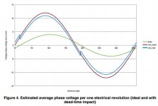
Also, please note that the picture in post #42 shows load current (A) and not the average output voltage.
For my understanding, are you assuming a circuit that switches between three voltage levels, positive, negative and zero? Or between positive and negative, with a (near) zero level occuring only during a dead time during switching to prevent overlap current?
Assuming it's three level, does that mean that for a small positive output signal, you switch between positive and zero with a very small duty cycle and for a very small negative output signal, you switch between negative and zero with a very small duty cycle?
Assuming it's three level, does that mean that for a small positive output signal, you switch between positive and zero with a very small duty cycle and for a very small negative output signal, you switch between negative and zero with a very small duty cycle?
I'm assuming the regular two-levels namely Vdd and GND, and not multilevel.
Also, there's no middle level for inductive loads, due to the commutation currents flowing through the body diodes that instead result in Vdd/GND voltage levels, even during dead-time.
If load current is positive, the dead-time output is GND and if it's negative the dead-time output is Vdd. This causes a fixed pulse-width error whose sign is opposite to that of load current.
I_load > 0 => V_out < V_ideal
I_load < 0 => V_out > V_ideal
However, in both the above cases, the absolute value, | V_out - V_ideal | is equal to td / ts x (Vdd/2). But, by sensing the sign of load current, the modulator is also able to obtain the polarity of this already known error and therefore fully compensate for it.
I see. Isn't "fully compensate" a bit exaggerated, as you don't know the dead time accurately unless you exactly know the switching time of the MOSFETs?
The quantities 'td' and 'ts' in my eariler expressions are the dead-time and switching period (1/fs) of the modulation. For PWM, both ts and fs are constants. Dead-time is also often a fixed value inserted just before (or during) gate-drive. So, for PWM, both are known quantities and dead-time compensation is possible. Any error due to rise-time/fall-time are to be treated separately. In fact, there are a lot of papers that discuss this. For example,
S. G. Jeong and M. H. Park, “The analysis and compensation of dead-time effects in PWM inverters,” IEEE Trans. Ind. Electron., vol. 38, pp. 108–114, Apr. 1991. (I think dead-time compensation was first shown in this)
https://ieeexplore.ieee.org/document/995662 (later development)
S. G. Jeong and M. H. Park, “The analysis and compensation of dead-time effects in PWM inverters,” IEEE Trans. Ind. Electron., vol. 38, pp. 108–114, Apr. 1991. (I think dead-time compensation was first shown in this)
https://ieeexplore.ieee.org/document/995662 (later development)
Besides, if you look at the dead-time voltage error, you would find it to be a square-wave at fundamental frequency (same as load current). In order for the loop to clear this error without dead-time compensation, a large number of harmonics of this square-wave must fall within the control bandwidth of the amplifier (harder as one approaches 20kHz). And, if this error is already cleared by means of an internal mechanism, that is something that makes the job easier for the feedback loop, and I guess something, is much better than nothing, isn't it ?
Sure, I just wonder how one can get it good enough.
I mean, suppose you have a two times 100 W class-D amplifier driving 90 dB at 1 W, 1 m loudspeakers in a room with a 1 m reverberation radius. You then get a maximum sound pressure level of about 113 dB.
When you use that equipment to listen to soft music, you probably want this square wave-shaped distortion product to be below the threshold of audibility, which is around -7 dB SPL at frequencies of a few kilohertz for young people with good hearing. So all in all, this square wave has to be attenuated to about -120 dB with respect to the maximum signal level, or maybe -100 dB if you count on masking by background sounds.
Still, class-D amplifiers that sound reasonably well at low sound levels exist, some even work open loop and they have been around for decades while your oldest literature reference is from 1991. It doesn't seem to add up, so I'm probably missing something.
There are vaguely similar problems with things I am much more familiar with; you also have dead zones or even hysteresis loops in things such as class-B amplifiers, tape recorders and sigma-delta modulators. There it is always solved with some sort of biasing (DC, HF or random a.k.a. dithering) to eliminate or overcome the nonlinearity, with or without negative feedback.
Last edited:
If your try working out the dead-time error magnitude for a 100V amplifier with a 40ns dead-time switching at 400kHz, you get something like (100/2)*40ns/2.5us = 0.8V, which is probably smaller than the ripple voltage itself, especially if you're operating at a high modulation index. This kind of error would be insufficient to cause audible distortion anyway.
Nevertheless, if the aim is Class-D that challenges linear amp performance, then every known error would have to be taken into consideration and improving the open-loop THD is almost always the starting point, since the closed-loop THD directly depends on it !
I assumed that the 1991 paper is earliest because:
a) I've heard so, while in academics (the "Park paper").
b) This paper does not cite any other articles on the same topic, which mostly indicates the non-availability of prior-art, as IEEE is usually very strict when it comes to making relevant references to existing work.
Now, there's also this 1988 conference paper that has the same title, is written by the same authors, and consists of almost the same content, but with fewer references when compared to 1991, if you're interested.
https://ieeexplore.ieee.org/document/665770
I think that what I was missing is the fact that at low signal levels, the sign of the load current is determined by the ripple rather than the signal, so you get an ultrasonic error rather than one at an audible frequency, except at very high volumes.
A 0.8 V peak-peak (is it peak-peak or peak?) square wave in the middle of the audio band in quiet surroundings would have been very audible: 20 mW of power into 8 ohm, so 73 dB SPL at 1 m with a 90 dB at 1 W, 1 m loudspeaker, and about the same at large distances in a reverberant room, typically around 76 dB SPL when it is a stereo system.
A 0.8 V peak-peak (is it peak-peak or peak?) square wave in the middle of the audio band in quiet surroundings would have been very audible: 20 mW of power into 8 ohm, so 73 dB SPL at 1 m with a 90 dB at 1 W, 1 m loudspeaker, and about the same at large distances in a reverberant room, typically around 76 dB SPL when it is a stereo system.
Maybe some comments from my side.
I would say almost all Audio-DACs or Digital-Class-D Amplifiers are based internally on a digital sigma-delta concept.
Directly after the I²S input there is typically an upsampling stage (basically feeding in 0's with a FIR filter behind) because internally the sigma-delta needs the same input-rate as output-rate. So if the output-rate of the sigma-delta is 768 kHz then the input fs must be also 768 kHz. Especially upsampling by power-of-2 factors (x4, x8, x16) are easier to implement in order to keep the whole system clock-synchronous. Therefore you also have such switching-frequencies like (384 kHz - basically 8*48 kHz).
In comparison to single-bit output sigma-delta converters, there are often "Multibit-Sigma-Delta" converters used. As you have instead of one bit more bits available, you don't need so high oversampling-ratios to get the same SNR at the output -> I think TI amps are having internally then 8-Bit output after the sigma-delta.
And now, depending if it is a usual DAC or a PWM based output there is even a current-steering array connected (also sometimes called afir -> analog-fir) or a PWM modulator.
The internal processing frequencies of the digital sigma-delta are usually not higher than 50MHz to 100MHz because the technology-nodes in which such IC's are developed are usually not allowing more (I think in the range of 100-300nm or so).
I published a basic I²S-to-PWM FPGA project on my private GitHub channel -> https://github.com/YetAnotherElectronicsChannel/FPGA-Class-D-Amplifier
It's definitely not the reference of audio performance but is showing the concept behind.
EDIT:
I have also seen designs where there is an ASRC directly behind the audio-input and all the internals (sigma-delta and modulator) working on a fixed-frequency driven by an external oscillator. This is especially useful when the input-clocks of the I²S are jittery (especially from SPDIF or so).
Last edited:
@ TNT: Cool! I had heard about it several years ago, but then it was still very much in development and under NDA. Nice that it has resulted in a product!
I have to return to my earlier question ... can you knowledgeable people see any real advantage of the "short-cut" and is so, what is the gain?
//
//
The advantage of having lots of loop gain and including the output filter in the loop are low distortion and a flat frequency response, even when you use cheap coils and when the load impedance is not exactly what you designed the output filter for (reactive loudspeaker instead of a purely resistive test load, for example).
Like the article says and confirming what newvirus2008 wrote on this thread, the people who worked on that amplifier found out they could more easily make a high-order loop with lots of loop gain if the loop filter was made digital. Hence they went for that approach. I guess it is also more easily adaptable to different output stages and filter parameters.
Like the article says and confirming what newvirus2008 wrote on this thread, the people who worked on that amplifier found out they could more easily make a high-order loop with lots of loop gain if the loop filter was made digital. Hence they went for that approach. I guess it is also more easily adaptable to different output stages and filter parameters.
- Home
- Amplifiers
- Class D
- PCM to PWM conversion 101