I was just comparing these to other boards they made for me that came in the same shipment, and the others are all tinned. Like I say, I wouldn't care, but shouldn't the bare copper plate-through have the added protection of being sealed off in some way? And certainly the added layer would decrease any resistance through the VIAs, right? maybe I'm overthinking this.
You can dab solder into them but I think solder is higher resistance than the actual plating so it wouldn't have any advantage unless it's high current. Possibly corrosion may be an issue. That's why I have mine covered in soldermask. A layer of Humiseal would take care of that too.
What are you using the vias for? Cable connections? test points? My worry would be without the plating to "sandwich" any solder, there's a chance they could loosen over time, particularly if the board / wire is subject to vibrations.
--snip--
edit: silly question but could your software have produced non-plated vias? Do the gerber files have plates around the vias?
These vias have only one function, to join traces from solder side to component side. My actual terminal connections where wirers are connected have wider holes, and they are all tinned fine. As far as my software, it does provide for non PLATED holes, and even makes a separate drill file with the words "unplated holes" in the filename. But plating was a poor choice of words in my diagram. The plating is there, just not the tinning (and I have to wonder by what magic they were able to NOT tin the vias, even though all the other plated holes were tinned.
How is the via (aperture) specified in your gerber data?
pad stack top pad, top solder mask,finished hole size.
Looks to me like the top solder mask is around the finished hole size or some where in between the fhs and the pad.
This is fine, the only time you want an exposed via pad is for probing/test. Covering vias with solder mask has the advantage of improving yield, if there is a wave solder operation.
So amid all the raves about PCBWAY, I have to report some bad experiences too. The lack of HASL covering on the vias in one of my orders (which I described a few posts back) were not a big deal, but definitely it was their error. The proof was that side by side with another PCB done in the same order, the vias were all coated. The bigger issue I had was that several small holes ( all of a certain size) were not drilled all the way through the boards. Fortunately these were non electrical holes which I place in the center of some components to "line up" a board with a control panel. But it was a mistake just the same. Once again the same size holes in another board they did were done properly. Obviously a drill defect in the machine used to make the apertures in first board.
There was also another board which was a purely mechanical board (no traces, just holes and black silkscreen). It was to be used for a control panel, so I specifically instructed them to not add anything to the existing silkscreen. They ignored that instruction, adding the order number to the silkscreen, leaving me with less than ideal panels.
All companies make mistakes eventually. Thats not a big deal. But the test of a relationship, whether business or personal, is how things are handled when mistakes are made. In this case I asked for the boards to be redone correctly. In fact I even offered to furnish newer files (since my designs are always being tweaked anyway) if they would just give me a discount, but if not just re-doing the existing boards was fine too. The result? The representative told he would "push" his manager for a discount, but did not know whether "it could be done". Beyond that all I basically got was a "sorry". Despite numerous marked up photos and explanations, at no point was any error admitted to, nor any responsibility taken.
So all this to say, I'd still say PCBway is still a great boon to all of us DIY folks on a budget. But beware. If you're boards are less than perfect sometiems and you want/expect them to stand behind their work, don't be surprised if all you get is "sorry". And for anything in the "special" category (like my control panel), I wouldn't mind spending a little more just to have a representative that both speaks English well, AND takes the time to READ and ADDRESS more than one sentence per email.
I just curious. Have you checked you files on the boards with no HASL on the vias? Were they covered by soldermask?
They must produce a staggering number of boards in a day to make any money so I can see why they would put an ID number on your boards. How would they keep track of what board goes where otherwise?
You are asking Chinese people to produce a product for you. Common courtesy would be to address them in their language. Why are you emailing them requests? The whole process is automated. It doesn't matter what language they speak. Any time you select human interaction over a machine you are asking for trouble.
I've seen a couple mistakes from them first hand and thought they handled them very well. The mistakenly sent me some boards that were supposed to be sent to a fellow in California. I had received an order the previous day and somehow my shipping invoice became attached to this other orders packaging. They reimbursed me for duties I had paid and had me ship them out express post to the correct address. Shipping likely cost them more than a replacement set of boards. Their only concern was getting the boards to the correct address as quickly as possible.
On another order they missed drilling 4 large holes in a set of boards. I brought it to their attention just to let them know there was an issue but told them I would fix it myself. In about a minute I had the whole set of boards repaired. They reproduced the boards anyway and are waiting to ship with my next order.
Different sales reps may handle issues in different ways there. Daphne has handled any interaction I've had with them and I have to say I'm very happy with any dealings I've had so far.
Thx jwilhelm,
for your assessment of a cut cost pcb fab shop run in Asia. Both accounts sound accurate, informative and what I would expect.
They have a process and stick to it, they have to, special processing just slows down the whole process. For all we know, the silk ID add, could have been put on automatically during DRC and panel prep.
The last thing they would do, is read my fab/control drawing, what is that 🙂 Do they even ask for one in the upload reqs?
For what you get, I would let them fab a 2-layer pcb for me, with min 10/10 mil line/spc and 20mil fhs, that is it, to start with. We call it PC10 tech at HP back in the 90's.
For a shop like this, all your holes should be plated, even if they have no connectivity. Unplated holes are done at the end of the process, , it is the panel put back on the drill machine again, for a second time. This is done, just before s/m & s/s. It detracts them from their normal processing. BTW, pcb assembly tooling holes are NOT to be plated, as the tolerance is less on PTH = BAD.
Last edited:
There is no fab control drawing required. They just produce boards directly from Gerber/Excellion files which is all that should be expected from them. All the information should be in the files anyway.
The order they mistakenly shipped to me was for 4 layer boards. It looked like 10/10 mil and actually looked pretty good. Automated processes are remarkable these days. Much nicer than the hand etched crap I used up until 6 months ago. I can't remember if it was them or Iteadstudio that said minimum trace width was 7 mil. Either way it's much finer than required for audio or even a DAC.
The order they mistakenly shipped to me was for 4 layer boards. It looked like 10/10 mil and actually looked pretty good. Automated processes are remarkable these days. Much nicer than the hand etched crap I used up until 6 months ago. I can't remember if it was them or Iteadstudio that said minimum trace width was 7 mil. Either way it's much finer than required for audio or even a DAC.
I could not say it any better, PTH/smobc, all the way!!Much nicer than the hand etched crap I used up until 6 months ago.
I stick to 8/8/16-20 mil fhs unless I am doing something special.
A little pcb history for you, since this is what I did "pcb design" for many years, from tape to CAD/CAM 🙂
We did 5/5/12 mil fhs back in the 90's at HP, 4/4/8 mil fhs was special order, sent to the HP/PRC division in Germany (the best of the best). Our simplest pcb was done in 4-layer back then. Having a dedicated Vcc/GND plane is great to work with. Makes the regulatory/EMI EE, a happy man 🙂 because it makes for a lot quieter design. Multi-layer is not so much of a premium these days.
Last pro pcb I/we did at McDATA "~2003" was 16 layers, in 62 mil (parallel PCI bus). It was a Fibre Channel 2/10Gb/s test card that ran in a PC. 314 8mil, 6571 10 mil,354 16 mil vias, zbc/106 2 mil cores, Immersion Au, 1152 BGA Xilinx and a slew of other goodies 🙂 The pcb shop was Pro-Tech. Assembled at SCI/Samina.
I managed to get a blank pcb. Maybe I can show you one day, it is a thing of beauty, you can make out objects looking through all the vias in the 1152 BGA breakout pattern.
Even though we had the CCT Spectra router, most of the layout was done by hand. We did modeling, parasitic extraction and simulation of the transmission lines using IBIS models. I big effort, for a big team, but success on the first rev.
Any other good and cheap board house other than PCBway?
I'm actually working with a former employee of PCBWAY as I write, who is starting up his own business. I wouldn't be surprised if the resources he uses are the same, but I've worked with him in the past (when he was still at PCBWAY) and our communication was much better. That in itself should make a huge difference, as will standing behind his work. Prices so far seem about the same. I can't honestly recommend it yet, but I'm going to give him a chance with some boards and will offer a review when my first order is done.
I just curious. Have you checked you files on the boards with no HASL on the vias? Were they covered by soldermask?
Actually the issue wasn't solder mask, but a lack of HASL covering on some vias. I also had some other holes not completely drilled through.
Different sales reps may handle issues in different ways there. Daphne has handled any interaction I've had with them and I have to say I'm very happy with any dealings I've had so far.
Thats likely the most important thing.. perhaps i will directly ask for Daphne and see if the communication is better.
If solder mask is covering the vias in the software, there will be no HASL on them. The software is the most important form of communication if you hope to achieve a usable end product with any sort of automated manufacturing.
As for drill holes not being completely through I don't think it's possible to specify that in any pcb software so they should definitely fix that for you.
I'll pm Daphne's email address to you when I get to my computer.
As for drill holes not being completely through I don't think it's possible to specify that in any pcb software so they should definitely fix that for you.
I'll pm Daphne's email address to you when I get to my computer.
Last edited:
If solder mask is covering the vias in the software, there will be no HASL on them. The software is the most important form of communication if you hope to achieve a usable end product with any sort of automated manufacturing.
As for drill holes not being completely through I don't think it's possible to specify that in any pcb software so they should definitely fix that for you.
I'll pm Daphne's email address to you when I get to my computer.
Please resend that email? I had the email and for some reason it got clobbered. Thanks!
If solder mask is covering the vias in the software, there will be no HASL on them. The software is the most important form of communication if you hope to achieve a usable end product with any sort of automated manufacturing.
As for drill holes not being completely through I don't think it's possible to specify that in any pcb software so they should definitely fix that for you.
I'll pm Daphne's email address to you when I get to my computer.
So writing to Daphne was immensely more helpful. She looked into the problems I described. On one (the half drilled holes) she clearly apologized and said it was their fault, on another (The id in the silkscreen) she explained how i should better describe this as unwanted in my text instructions. Finally, she explained that my software did indeed specify that my vias should not have the HASL layer, just on that board. Very odd, but OK... at least its explained.
There was no offer to re-do the board with the missing holes, and I didn't press the issue as it was something I could live with. But I was happy enough to find someone that could at least look into the matter, and take some responsibility for a mishap that were was fault, and actually addressed all the points in my email.
Bottom line, if you work with them and get a different rep, and feel you are having trouble communicating or getting a request addressed, Daphne might be a good person to ask for.
PCBWay has another portal facing Chinese customers:
http://www.jdbpcb.com/online/
Quotes from the local portal is cheaper (tried a few online quotes, between 15% to 33% cheaper depending on config) than pcbway.com, but it only deliver orders in China.
For those who have friends living in China and don't mind doing the forwarding, it could generate some savings.
Last edited:
PCBWay - more experience with ordering
I have ordered some board 3 weeks ago, production time 3-4 days and shipping via DHL express within another max. 7 days. First, the haven't booked my instant PayPal payment for a week, they did it after I asked why they haven't start production yet... 2 days later my boards were finished and the status changed to "delivery ready". But then, the status didn't change again for 4 days and I asked when they would ship my items. They answered me, DHL lost my package, but I could get my money back. But I want my boards, I'm not working several weeks just for fun. Okay, they promised me, to produce my boards again immediately and send them out asap. This is 3 days ago. Again no status change, no email contact, nothing. I cancelled my PayPal payment today. Never again with these Chinese Rip-Offs.
I have ordered some board 3 weeks ago, production time 3-4 days and shipping via DHL express within another max. 7 days. First, the haven't booked my instant PayPal payment for a week, they did it after I asked why they haven't start production yet... 2 days later my boards were finished and the status changed to "delivery ready". But then, the status didn't change again for 4 days and I asked when they would ship my items. They answered me, DHL lost my package, but I could get my money back. But I want my boards, I'm not working several weeks just for fun. Okay, they promised me, to produce my boards again immediately and send them out asap. This is 3 days ago. Again no status change, no email contact, nothing. I cancelled my PayPal payment today. Never again with these Chinese Rip-Offs.
I used PCBWay (also called 3PCB) for some 36x90mm 4-layer w/ ENIG automotive radio pre-amp boards (pulling the audio signal straight from the DSP's DAC outputs and then gaining/buffering/LPF'ing it to be used with an aftermarket amp's RCA inputs). The quality was good and I did not observe any defects in the vias or etching. I did not need to deal with their customer service reps since all of the automated stuff worked properly. Here are some links with my posts on another forum that show the boards up-close:
http://www.r3vlimited.com/board/showpost.php?p=4312001&postcount=50
http://www.r3vlimited.com/board/showpost.php?p=4314455&postcount=58
Right now, I have a 4-layer design, 40x80mm w/ ENIG, that is being reviewed by their people and I should be paying for work to begin tomorrow if they don't have any questions. There are 120 plated vias in the thing (0.3mm diameter hole, 0.625mm diameter pad). Minimum trace width is 0.18mm (7mil) and minimum spacing is 0.20mm (8mil). So, hopefully I will have these in-hand in a couple of weeks and I'll try to remember to report back on the quality. Hopefully there are no electrical faults, because this thing is going to be doing signal processing for a critical engine management subsystem in my car!
Last edited:
I'm on my 8th batch of boards with good success from them. I ordered a bunch of SMT boards from them 2 batches ago but I cheaped out and ordered HASL with lead. Your gold plated boards are much better around the pads. The silk was a little rough on mine.I used PCBWay (also called 3PCB) for some 36x90mm 4-layer w/ ENIG automotive radio pre-amp boards (pulling the audio signal straight from the DSP's DAC outputs and then gaining/buffering/LPF'ing it to be used with an aftermarket amp's RCA inputs). The quality was good and I did not observe any defects in the vias or etching. I did not need to deal with their customer service reps since all of the automated stuff worked properly. Here are some links with my posts on another forum that show the boards up-close:
R3VLimited Forums - View Single Post - RMT200 Tear-Down and Modifications Thread
R3VLimited Forums - View Single Post - RMT200 Tear-Down and Modifications Thread
Right now, I have a 4-layer design, 40x80mm w/ ENIG, that is being reviewed by their people and I should be paying for work to begin tomorrow if they don't have any questions. There are 120 plated vias in the thing (0.3mm diameter hole, 0.625mm diameter pad). Minimum trace width is 0.18mm (7mil) and minimum spacing is 0.20mm (8mil). So, hopefully I will have these in-hand in a couple of weeks and I'll try to remember to report back on the quality. Hopefully there are no electrical faults, because this thing is going to be doing signal processing for a critical engine management subsystem in my car!
Do you hand solder your SMT or do you reflow in an oven? I tried reflowing mine and the silk browned on me.
Yeah, I generally go for ENIG over HASL. Everything is generally cleaner that way and it seems to be worth the small extra cost to me.
I hand solder all of the SMT stuff. A future project of mine will be to build a PID controller into a toaster oven and use that for reflow, but for now it's all the "hard way"! Although I can do 0402 and TSSOP packages without too much trouble, I try to stick with 0603 and SOIC parts as much as possible since those are super easy in comparison.
I hand solder all of the SMT stuff. A future project of mine will be to build a PID controller into a toaster oven and use that for reflow, but for now it's all the "hard way"! Although I can do 0402 and TSSOP packages without too much trouble, I try to stick with 0603 and SOIC parts as much as possible since those are super easy in comparison.
Last edited:
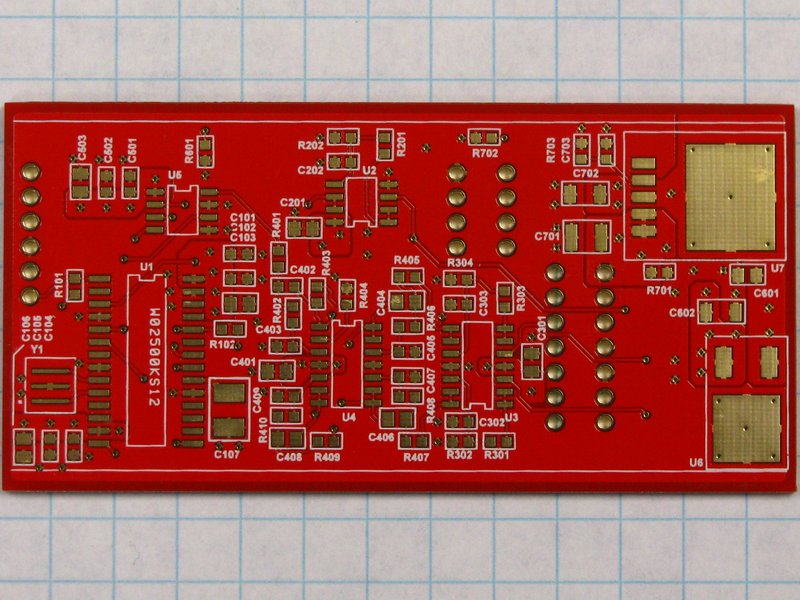
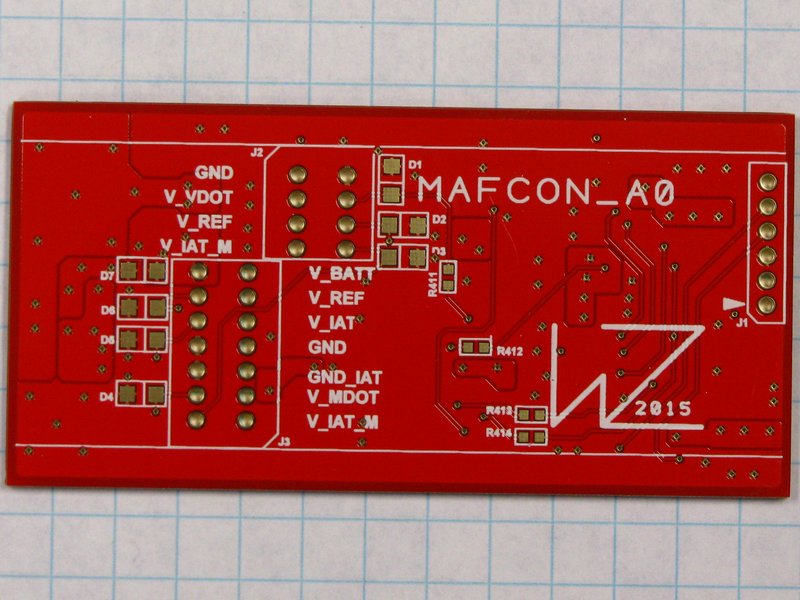
So, I placed an order for some 4 layer boards, 40x80mm with ENIG finishing, red soldermask and double sided silkscreen on May 15. The boards arrived today, the 22nd. Not bad at all!
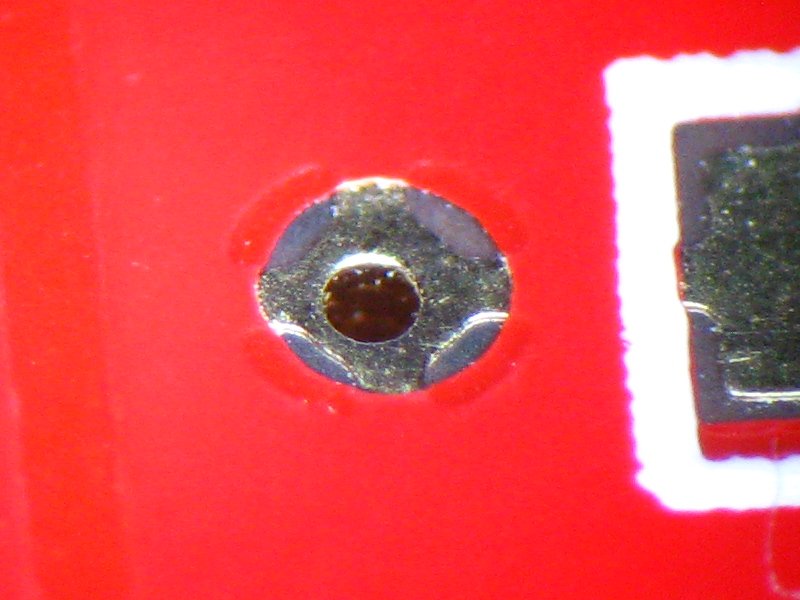
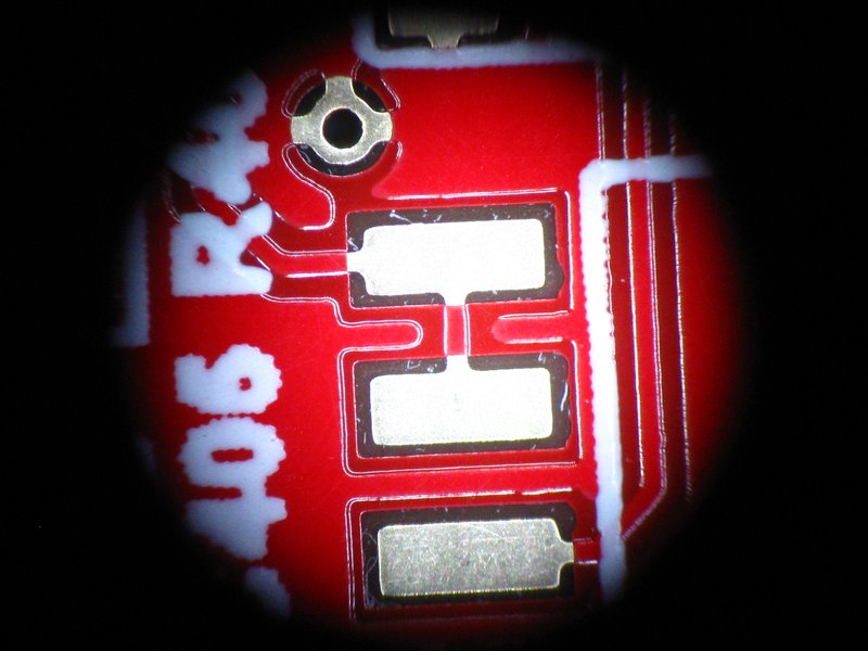
Overall I am happy with the quality. 4 of the 10 boards have slight scuffing on one of the big pads for a DDPAK regulator, but it is only cosmetic as far as I can tell under a microscope.
(here's the one with the worst scuffing)
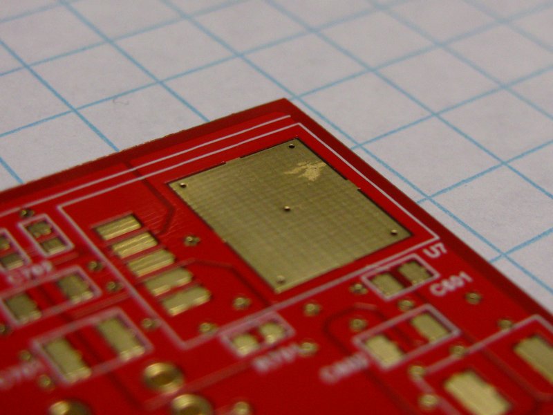
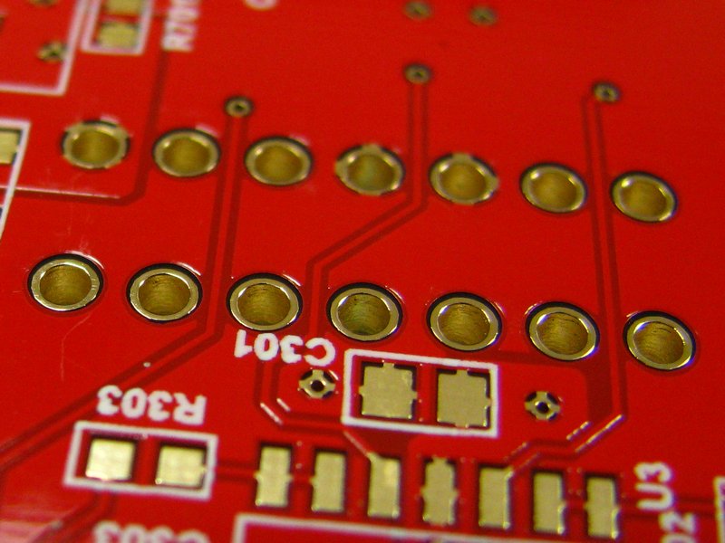
I have not gone through and inspected all of the plated holes & vias, but a quick spot check shows them to all be looking fine.
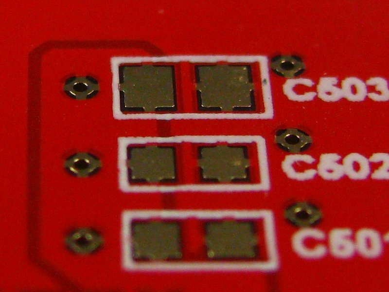
All of the fine details seem to have come through in the copper etching, and the soldermask application looked properly aligned (a previous project had 2 of the 25 boards with the soldermask offset enough to slightly overlap SMD pads). Having the copper ground plane fit between 1.27mm-spaced SOIC pads and 0603 passives was not a problem.
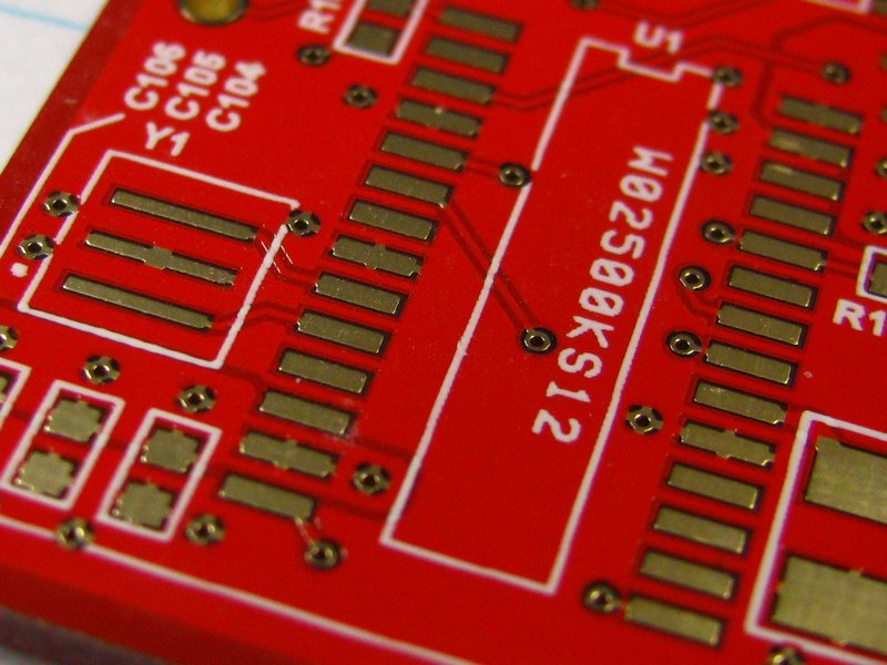
Overall I think that the boards look good. The total for this order, including shipping and fees, was $107. That is very reasonable for 10x 4 layer boards with ENIG and the initial assessment of quality that I have given these.
Overall I am happy with the quality. 4 of the 10 boards have slight scuffing on one of the big pads for a DDPAK regulator, but it is only cosmetic as far as I can tell under a microscope.
(here's the one with the worst scuffing)
I have not gone through and inspected all of the plated holes & vias, but a quick spot check shows them to all be looking fine.
All of the fine details seem to have come through in the copper etching, and the soldermask application looked properly aligned (a previous project had 2 of the 25 boards with the soldermask offset enough to slightly overlap SMD pads). Having the copper ground plane fit between 1.27mm-spaced SOIC pads and 0603 passives was not a problem.
Overall I think that the boards look good. The total for this order, including shipping and fees, was $107. That is very reasonable for 10x 4 layer boards with ENIG and the initial assessment of quality that I have given these.
- Status
- Not open for further replies.
- Home
- Design & Build
- Parts
- PCBway Ordering Experiences