You could go 4 layers and take advantage of the FR4 10kV/mm?
Define the mounting holes with the washer outline so you could see how close hot traces are. And why a metal hole?
Jean-Paul
JP
Define the mounting holes with the washer outline so you could see how close hot traces are. And why a metal hole?
Jean-Paul
JP
4 layers for mains boards?!?! I would never consider that to be honest. What will it bring?
Last edited:
Yes! L and N on inner layer so isolated and creepage could be reduced.
I´ve done this in a lot of power supplies.
JP
I´ve done this in a lot of power supplies.
JP
Being used to higher AC and DC voltages I am concerned about creepage but less so with 230V AC mains voltage often limited to 16A. Even 4 mm never caused me trouble. Now we are in the EU so relatively troublefree issues must of course be exaggerated to prevent being busy with real problems 😀
Last edited:
Aha! Now we enter PCB ordering territory! Up till now, the least expensive option I have found is DigiKey’s red PCBs with a fixed 1,6mm thickness and 1oz copper. But only two layers.You could go 4 layers and take advantage of the FR4 10kV/mm?
Define the mounting holes with the washer outline so you could see how close hot traces are. And why a metal hole?
Jean-Paul
JP
Still, if I limit this design to 1A applications, will this be less critical? 4 layer PCBs or 2oz traces or 2 mm thickness are really much more expensive.
The mounting holes is a good question, all PCBs I have ever stuffed have those rings around even if they are not connected to PCB ground. They are 3mm drills with 6mm outer diameter. Originally I placed them closer to the edges, but then I measured the PCBs I have here and they all have about 3mm clearance to the outer rim, so, 6mm from edge to hole center. Does this seem excesive?
Rafa.
Last edited:
I would need to change to kiCad perhaps?
If you do that, download one of the nightly builds. I've been running KiCAD 5.99 for a few weeks now. It has a few quirks/bugs (it's a beta version!) but seems stable.
There are many UI changes in KiCAD 6 vs KiCAD 5, so if you're going to learn from scratch it would make sense to start with the new interface.
I'm not saying you should move to KiCAD. Only that I suggest going with the new version if you do choose to go that route.
Tom
Aha! Now we enter PCB ordering territory! Up till now, the least expensive option I have found is DigiKey’s red PCBs with a fixed 1,6mm thickness and 1oz copper. But only two layers.
That's probably the lowest cost option, but at least for now it only works if you're within the US. For others there's OSH Park: OSH Park ~
Still, if I limit this design to 1A applications, will this be less critical? 4 layer PCBs or 2oz traces or 2 mm thickness are really much more expensive.
You don't need any of those. 1 oz (35 um) copper, 1.6 mm FR-4, two layers is plenty.
The mounting holes is a good question, all PCBs I have ever stuffed have those rings around even if they are not connected to PCB ground. They are 3mm drills with 6mm outer diameter. Originally I placed them closer to the edges, but then I measured the PCBs I have here and they all have about 3mm clearance to the outer rim, so, 6mm from edge to hole center. Does this seem excesive?
Seems reasonable. I usually place 3.2 mm diameter holes 5.08 mm (0.2") from the board edge. I would size the silk screen markings such that it's slightly beyond the head of the machine screws you plan to use. Usually M3 screws have heads that are 5.7 mm in diameter, so 6 mm sounds good. If you plan to use washers note that the cheap M3 washers are typically 7 mm in diameter. The washer will be connected to chassis, so watch the clearance and creepage around it.
Tom
We don´t need 4 layers!
JP
This is somewhat contradictory with previous posts 🙂
BTW in post #21 you ask why the hole in the PCB is metallized. I also do this for higher mechanical strength and the PCB will not be damaged as easily by tightening the screws. It is then (always really) a good idea to keep distance between the metallized hole and PCB tracks. In the given example clearance is by far not enough as you indicated. Having the holes not metallized through looks less OK, makes the board more easily damaged by the screws and since the metal screw and metal washer are there anyway (probably screwed in a metal standoff connected to chassis = PE) the clearances still should be enough.
The mounting holes is a good question, all PCBs I have ever stuffed have those rings around even if they are not connected to PCB ground. They are 3mm drills with 6mm outer diameter. Originally I placed them closer to the edges, but then I measured the PCBs I have here and they all have about 3mm clearance to the outer rim, so, 6mm from edge to hole center. Does this seem excessive?
Rafa.
Either you or I make a thinking mistake. I think what JPS64 means and writes ("Define the mounting holes with the washer outline so you could see how close hot traces are") is the distance between the metallized hole and the PCB tracks carrying mains voltage, in jargon "hot traces". Specifically the mounting hole in the right lower corner. Just suppose you use a galvanized steel M3 bolt and washer and a metal standoff. Then the hole is connected to PE. Then clearance should be changed according regulations.
Attachments

Last edited:
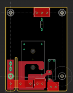
Thanks all... good catch on the mounting holes. I have added a 7mm silkscreen print so we can "see" what area the washers would cover, and I have increased the clearance for the washers to 2mm around the 6mm outer diameter. I have done that for the "daughter" PCB as well, as it had the smaller sizes and limits.
I have also kind-of implemented JPs idea on the bottom of the Mains PCB and the "hot" traces. I still think that you cheated on the 3 pin block, as I don't think there is one with such "nice" separations! 🙂.
My new traces are 5mm thick. I put the values through an online calculator and I only need them 7mm for 10A of current. If I lower the requirements to 1A, the 3mm traces seem to be enough. I have provisioned now for 5mm traces on most places, but I'm unsure how to do the terminations. For example, on the PSU paths, the 7mm on the trace would actually touch the other pad. So, I have done what seemed the "right" solution for such scenarios.
The PCB is now really big for such a little amount of components, I don't know how you guys make PCBs so small, mine is now bordering "huge" sizes.
Still, do you guys think this is, more or less, moving in the right direction, or am I just going in circles without improving anything with the changes I have made?
So, here are the new PCB layouts:
Mains Board


Logic Board


Thanks once more!
Rafa.
I have also kind-of implemented JPs idea on the bottom of the Mains PCB and the "hot" traces. I still think that you cheated on the 3 pin block, as I don't think there is one with such "nice" separations! 🙂.
My new traces are 5mm thick. I put the values through an online calculator and I only need them 7mm for 10A of current. If I lower the requirements to 1A, the 3mm traces seem to be enough. I have provisioned now for 5mm traces on most places, but I'm unsure how to do the terminations. For example, on the PSU paths, the 7mm on the trace would actually touch the other pad. So, I have done what seemed the "right" solution for such scenarios.
The PCB is now really big for such a little amount of components, I don't know how you guys make PCBs so small, mine is now bordering "huge" sizes.
Still, do you guys think this is, more or less, moving in the right direction, or am I just going in circles without improving anything with the changes I have made?
So, here are the new PCB layouts:
Mains Board
Logic Board
Thanks once more!
Rafa.
Rafa, L or N to châssis has to be increase! EU, > 7mm!
Isn't it funny? I interpreted this message as "L to chassis SPACING (clearance) has to be 7mm! N to chassis SPACING (clearance) has to be 7mm!"
I did NOT interpret it as "trace width has to be 7mm!".
You need 7 mm clearance distance from N(eutral) to chassis on the connector too. One way to do this is to use a 4-pin terminal with 5.08 mm pin pitch and skip a pin. Make the pad on the skipped pin smaller than the rest.
Why not fit all the components on the same board?
Tom
Why not fit all the components on the same board?
Tom
Last edited:
You need 7 mm (or 6.3 mm, depending on the standard) from any metal connected to the mains and the chassis for Class II electrical safety.My new traces are 5mm thick. I put the values through an online calculator and I only need them 7mm for 10A of current.
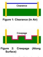
You'll come across two terms in the standards: Creepage and clearance. I've attached a figure to explain them.
The traces should be wide enough to carry the current, but that's a separate issue.
Tom
Attachments
Ok, so I take it I need both a 7mm trace AND a 7mm space between traces? Or I need to dial down the trace and increase the spacing?
I’m confused. Since English is not my main language, I ask for some leniency here.
So, was it OK to have 3mm traces but I need to increase the spacing between traces?
Thanks for the clarification.
I’m confused. Since English is not my main language, I ask for some leniency here.
So, was it OK to have 3mm traces but I need to increase the spacing between traces?
Thanks for the clarification.
You need 7 mm space between anything L/N/PE/chassis and can do with less than 7 mm wide PCB traces. Always think of worst case scenario so what currents can occur with a short circuit. The temptation could be to have thin PCB traces to win space but those could act as a fuse when a short occurs. As explained you can make it easier by using a PCB mount IEC inlet.
BTW connectors are usually right at the side of the PCB. No need for a few mm PCB material extra. You can easily add the 555 circuit to the same PCB and skip 2 mounting holes (why 6 of them?).
If you swap the PCB tracks to AC/L and AC/N of the IRM-03-12 the board will be better. Mains voltages are not polarized AFAIK and now the PCB tracks/traces are crossing each other 🙂
Last edited:
Thanks jean-paul.
Could you guys then please help me understand then: with those regulations, the Relay does not comply as the distance between it's pins is 5.04mm. So, any trace that comes in contact with any pad on the relay is already closer than 7mm. So this relay cannot be used to interrupt mains?
Thanks once more,
Rafa.
Attachments

Isn't the 7 mm clearance requirement technically between anything the user can touch (so the chassis and anything that connects to it) and L (live), N (neutral) of the mains? I don't believe you need 7 mm between L and N, and also not between L and "switched L", so the relay is OK. No?
There's a separate requirement for trace spacing, but that depends on the voltage and not so much on Class II electrical safety as I understand it.
There's yet another standard for disconnect switches which dictates contact spacing, but that's a separate issue. One can get around that issue by providing an IEC inlet and instructions that the power isn't considered fully off until the power cord has been unplugged.
Tom
- Home
- Amplifiers
- Power Supplies
- PCB: Push on / Push off Mains Switch