1/4" quick disconnect solder in tabs...if your interested
https://www.ebay.com/itm/2950041965...4BEQHmBQEe&var=&widget_ver=artemis&media=COPY
https://www.ebay.com/itm/2950041965...4BEQHmBQEe&var=&widget_ver=artemis&media=COPY
as I previously said, this first board experiment is only representative and to get familiar with kiCad. I still have to understand how many objects are available and how many will be useful for the real crossover I want to get to. this board will be assembled with what is available at home, making the board myself. nothing stops me from using faston connectors. (which I can't find on kiCad) for my diy board, I will use a 0.5mm copper sheet and I'm understanding from everyone that it is very important to avoid tracks that are too small. and it is obviously correct that little copper is not the best.
if I have to be honest I still have trouble finding the elements to use in kiCad. the positive thing is that having experience in using different graphic and structural design programs, I know where to put my hands even in the project files of many programs.
one thing is still not clear to me, the pads... are they created automatically or is it better to delimit them by hand? do the pads change the path of the signal and interfere negatively with the frequency cuts and attenuations?
Ahhh, gotcha. Once I know what the part is, I create a "footprint" in KiCad for it. There you can define all the solder pad dimensions and such. You can also modify existing footprints, as well as change pads and such by right click editing parameters.
There is no accounting for taste, some individuals find a well executed crossover aesthetically pleasing.Still having parts externally has no benefit (outside test phase). It is ergonomically and esthetically poor practice and generally not appreciated by anyone else except the builder/owner.
Two potential acoustic benefits of external crossover mounting:
At high power levels, crossover resistors and coils can get quite hot, external mounting keeps that heat out of the speaker cabinet, reducing "thermal compression" and crossover shifts due to voice coil impedance rising.
I've seen burnt fiberglass circuit boards under resistors, and melted coil bobbins in pro PA cabinets with surviving loudspeakers.
Art
@jean-paul
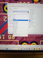
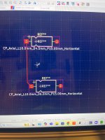
I tried to insert the footprints directly from pcb editor. I would like to understand from you how you do it if then with the problem < no net > by joining the tracks it is all an error. How do you solve this thing?
I tried to insert the footprints directly from pcb editor. I would like to understand from you how you do it if then with the problem < no net > by joining the tracks it is all an error. How do you solve this thing?
🙂 certainly this. but when you don't have a schematic upstream, how can you manually force a trace?
If whatever your connecting has the same net name, you should be able to connect with a trace. See what each pad is defined as.
It's definitely my mistake because I hadn't created the netlist with all the components and therefore the capacitor where I have to connect doesn't appear in the entries (net).
Huh, yeah, I don't know? I'm by no means a wizz at KiCad, hopefully someone else can shed some light on it.
It really should be that simple.
It really should be that simple.
wait, i just tried it and it works if you place two new ones. the problem is if i have to connect the two new ones to others that had a netlist. another strange thing is when you have to create a zone and they are not all on the same level. a real mess!
😱😉
😱😉
Ok, not understanding, if you have a net list, you should be able to define a pad of a component to a net list label.
For custom speakers I do not use PCBs. I prefer to glue the components to fiber board and direct wire them.
- Home
- Loudspeakers
- Multi-Way
- PCB or not PCB, this is a problem


