So what you are saying is that things like loop area or component placement don't make a difference, just connecting the dots is all that is required.
Don't know where you got that idea from, I never said anything of the sort.
Please find me more examples of via stitching used in fence-like lines specifically around the input signal traces of an amp. This is the very specific thing I was referring to. I would appreciate it. I actually don't see very many examples of stitching used in hifi analog audio components.
You probably won't find many audio circuits with via style fencings given it has limited effectiveness, this is why you see them used in high speed digital and RF circuits. "Via Fence - A term for the ground vias that are placed along the length of a controlled impedance line to isolate the sensitive circuit from the aggressively noisy circuits."
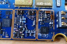
As far as I can tell it looks like the via's in the Hegel preamp might be only stiching the top and bottom ground planes for the copper between the center and outer conductors on the pcb for the rca connectors from the rear panel to the switching relays.
Just trying to understand what you mean by not needing any creativity.Don't know where you got that idea from, I never said anything of the sort.
Here is somebody with a distinct layout style:
My first GB
Just trying to understand what you mean by not needing any creativity.
Here is somebody with a distinct layout style:
My first GB
I bet manufacturers love all those holes to drill. It must be time consuming.
That many holes must weaken the structure of the pcb.
Interesting enough to embed in the forum.
Once you see it, it is "obvious". However it was not obvious until the price of 2-side and vias dropped to "zero".
I know a 1972 PCB tube amp where the on-board AC heat badly corrupted the signal. "Via-twisted" heater runs would have fixed that; but >$1k back in those days.
Attachments
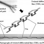
I‘m using this technique for heather supplies for tubes since 20 years! Twisted pair power routing.
Nice to know that study existing.
JP
Nice to know that study existing.
JP
Lots of talking past each other -- in a literal sense, yes, there are series of best-practice methods to layout, but also an "art" (the creativity of the designer) to which compromises and the overall packaging. Nothing wrong with it being aesthetically pleasing, albeit this seems a case where form *should* follow function.
*Who am I kidding for a lot of fashion-audio products. But still...
*Who am I kidding for a lot of fashion-audio products. But still...
Lavardin with some fancy pattern on a one-layer board. I think it's decorative, or at least not the ground plane.
It might look pretty, but it has a very useful purpose, and shows some thought in the Design For Manufacturing (DFM) process. The pattern is called "Copper Thieving" and is done to balance the total area of copper on each side of the board, and to keep the percentage of copper VS unplated area roughly constant across the board area. This is more important as the board density goes up, and the hole size goes down. It's purpose is to evenly distribute the plating current across the board so that the plated through holes get plated evenly.
Copper thieving confusion - Let's clear that up | EE-Training
You probably won't find many audio circuits with via style fencings given it has limited effectiveness, this is why you see them used in high speed digital and RF circuits.
In most audio designs on a 2 layer board there are enough components connected to ground, such that the plated through holes that the components are placed in provide sufficient ground connections between the top and bottom layers.
In RF device boards the placement, density, and number of vias connecting the ground layers is more critical as the frequency goes up. Worse case is a device like a cell phone or two way radio where audio, digital, and multi band RF are all present in the same often tiny and dense PC board. In this case via fences are and separate ground planed for each domain are used to separate the digital, RF and audio domains. Often individual RF circuits are fenced off from each other. Similar techniques could be used to separate the audio and digital domains on a DAC board, especially if high S/N specs are going to be quoted.....do you really believe that a 110 dB S/N number can be achieved on a PC motherboard?
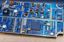
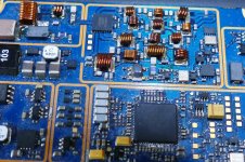
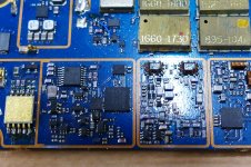
Here are some photos of a PC board I laid out about 12 years ago for a prototype two way radio. This is the RF board that mates with a separate digital / audio board, so there is no low level microphone audio on this board. There is 5 to 8 watts of RF power from 136 to 941 MHz, low level RF receiver signals in the less than 1 microvolt range, digital communication over SPI, I2C, digitized RF at 22 MHz, and a boost converter producing 28 volts at half an amp from a 6 to 10 volt battery pack.
This is a 10 layer High Density Interconnect (HDI) board. It has a conventional 6 layer layer core, with two additional thin outer layers of traces and vias photographically deposited onto a thin (1 to 2 mils) layer of material similar to the solder mask on each side. Very tiny 1 to 2 mil vias can be placed on these layers for very high density required for high pad count BGA chips.
Each subsection is fenced off from anything that could interfere with it, or to prevent interference to other subsections. After stuffing the board metal shield cans are soldered down on these tracks. They are not on these boards since these are prototypes for testing. Those are the gold tracks seen in the photographs. Very tiny via holes can be seen in these tracks tying all the outer layers together. There are lots more scattered throughout the board, but covered by the outer blue solder mask. You will see a few larger vias that tie all the grounds together on all 10 layers.
Most of the RF runners are on the outer HDI layer, or the outer conventional layers (not visible). The noisy digital buses are sandwiched between two ground planes in the middle of the board and heavily fenced to create "virtual coax cables" inside the board.
This was state of the art in 2008......the art has advanced a lot since then.
When laying out a simple audio board, especially one containing a power supply, the designer needs to consider all the current loops in the design and keep them separated, usually joining together at one point, often called the star ground. This is usually the negative terminal or common terminal (with split supplies) of the main filter cap(s).
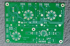
Here is a picture of my Tubelab SSE board from about the same time period as the radio board (2006). The grounds from either side are joined by through plated holes for component leads. The star ground point is the negative terminal of the big filter cap in the upper right on the back side of the board. There is a fat runner to the terminal connector on the right side. This is where the HV center tap on the power transformer is connected. The rectifier tube is below this. All of the noisy charging currents for the filter caps are constrained to this area, walled off by ground from the rest of the board. There are brief high current pulses topping off the filter caps on the peaks of each cycle at a 100 or 120 Hz rate. These must be kept out of the audio sections.
You will also see a fat ground trace going downward and left across the board to the input connectors, This is the return ground path for the signal input and driver section of the board.
There is also a fat trace extending leftward across the center of the board, it continues leftward on the front side of the board after passing through three parallel component holes.
Because of the high current the path mentioned above (C2 to R27 and R17) is duplicated on both sides of the board. This is the discharge path for the power supply capacitors through the OPT's and output tubes. B+ is routed to T3 (an OPT) on the top side of the board, and T2 on the bottom side of the board. The returns from the OPT's are routed to pin 3 of the output tubes, whose cathodes are connected to R27 and R17 then back to ground at the filter caps. This is the high current discharge path for the power supply. It is a separate loop from the charging path, meeting only at the "star ground" point. Keeping these two loops separated is key to low hum and freedom from oscillation.
The driver section has it's own separated loop from the power supply. There is a dedicated trace from the positive terminal of C2 to R24 and R14. This provided power to the CCS chips which feed the plates of the 12AT7 tube. The CCS chips provide a 60 dB reduction in residual hum, providing the driver tube with clean DC which flows back to the star ground through R20 and R10. This is a third separate current loop, again separated from the other two, meeting only at the main filter cap.
Heater current is a completely separate loop. Entering through a connector at the back of the board. It is biased to about 45 volts above ground by R4, R3 and C3. The ground tie point is to the fat trace that returns output tube current to the star ground. Do not connect this to anything near the input of the amp.
Mastering these techniques are key to making a good WORKING audio PC board (or a PTP design)....... the pretty ART is up to you.
Attachments
This is a 10 layer High Density Interconnect (HDI) board.
I can just about wrap my head around 2 layers. 10 layers is just pure wizardry!
Because is has influence on the Circuit
Because for certain PCB in Audio its very important that you select the way of Layout very well.
I have to redesign a PCB for a Class A the third time because of Capacitive Problems where the layout of two lines do falsify the output of the input Signal, creating Noise and generating not recoverable Errors like Hum, Noise, Oscillation, all stuff no one wants.
Make short, and where ever it's possible thin lines except when there is a lot of power passing through. If you need to draw long lines - over 10 cm in lengt to make them at least 2mm wide, and if these are Signal lines, stay away from lines which powers up the Board. because of inductive and capacitive noise generation which will occur on the board.
Make if possible a double Layer, if you can't do by yourself then let some shop do it for you. Use a top ground Plane if possible.
I make my double layer by myself. If you need help on that I have wrote some documentation on this some years ago. Can be uploaded here..
The most important thing is, work exactly and clean. If you use Positive Photo reactive PCB from Bangard or any manufacturer, be sure to read their instruction. DO NOT USE TRANSPARENT FILM when you print the LAYOUT with a LASER PRINTER.. I assure you, there will be a lot of Testing and wasted PCB's.
Use Transparent Drawing Paper this will work very well. Make sure that you put the PRINTED SIDE FACE DOWN on the PCB to Avoid Ghost images. After you printed the Layout, check the print if its really DARK BLACK . If you find parts of the print where you think that it needs to be better either print a second sheet and put it over the first one - or manually correct it using Black No Water soluble drawing Pen. Make sure that the PCB side is correct before you print Negative Positive..it's not the same if you look a the PCB "through the PCB" at the lines or if you Flip it.. and look it from Bottom.
May there is need of inverted Printing for double sided PCB. Otherwise when the PCB is finished you will not be able to place the parts as you wish if layout on the PCB is the wrong way around..
Check development Times of the developer you will use.
Check Water temp and amount of developer used with a Scale, which is accurate to at least 1Gramm/Kilo or better.
If you use ACID to Edge the lines, like Ferro3 or similar, make sure that you stand by there while its etching. Use Warm Water of about 50Degrees Celsius, this will speed up the edging and also give better results..From time to time shake the container with the acid that some Air gets into it, this will sure help to reduce etching time.
Documentation you can find on the internet if you want to know more than this or have any other question., all you need to do is to ask.
Hope this helps
Regards Chris
http://www.hecco.ch/pcb_double_sided.pdf
Why would a PCB need to have style or creativity? PCB layouts need to be functional to meet various engineering design criteria.
Because for certain PCB in Audio its very important that you select the way of Layout very well.
I have to redesign a PCB for a Class A the third time because of Capacitive Problems where the layout of two lines do falsify the output of the input Signal, creating Noise and generating not recoverable Errors like Hum, Noise, Oscillation, all stuff no one wants.
Make short, and where ever it's possible thin lines except when there is a lot of power passing through. If you need to draw long lines - over 10 cm in lengt to make them at least 2mm wide, and if these are Signal lines, stay away from lines which powers up the Board. because of inductive and capacitive noise generation which will occur on the board.
Make if possible a double Layer, if you can't do by yourself then let some shop do it for you. Use a top ground Plane if possible.
I make my double layer by myself. If you need help on that I have wrote some documentation on this some years ago. Can be uploaded here..
The most important thing is, work exactly and clean. If you use Positive Photo reactive PCB from Bangard or any manufacturer, be sure to read their instruction. DO NOT USE TRANSPARENT FILM when you print the LAYOUT with a LASER PRINTER.. I assure you, there will be a lot of Testing and wasted PCB's.
Use Transparent Drawing Paper this will work very well. Make sure that you put the PRINTED SIDE FACE DOWN on the PCB to Avoid Ghost images. After you printed the Layout, check the print if its really DARK BLACK . If you find parts of the print where you think that it needs to be better either print a second sheet and put it over the first one - or manually correct it using Black No Water soluble drawing Pen. Make sure that the PCB side is correct before you print Negative Positive..it's not the same if you look a the PCB "through the PCB" at the lines or if you Flip it.. and look it from Bottom.
May there is need of inverted Printing for double sided PCB. Otherwise when the PCB is finished you will not be able to place the parts as you wish if layout on the PCB is the wrong way around..
Check development Times of the developer you will use.
Check Water temp and amount of developer used with a Scale, which is accurate to at least 1Gramm/Kilo or better.
If you use ACID to Edge the lines, like Ferro3 or similar, make sure that you stand by there while its etching. Use Warm Water of about 50Degrees Celsius, this will speed up the edging and also give better results..From time to time shake the container with the acid that some Air gets into it, this will sure help to reduce etching time.
Documentation you can find on the internet if you want to know more than this or have any other question., all you need to do is to ask.
Hope this helps
Regards Chris
http://www.hecco.ch/pcb_double_sided.pdf
- Home
- Design & Build
- Construction Tips
- PCB Designs to Study