You won't believe it, but sometimes it makes sense to design amps that far exceed you hearing capabilities.
Why ?
I have all sorts of amplifiers here both self designed and bought in and they all sound pretty much the same.
Maybe the class A has a slight edge on the rest and sounds a little more detailed.
I am not going to dig deep into my pockets for something "better" where I cant hear the difference. That's just audio snobbery.
A properly laid out PCB need not be more expensive than a poor one, so why not do it properly, and what has digging into pockets got to do with it?
I think it is a misconception that anything that is inaudible is necessarily acceptable. Ideally the whole chain from microphone to loudspeaker should not have any audible distortion, so each piece of equipment in the chain has to have much less distortion than just below the threshold of audibility. It makes sense to keep most of the distortion budget for those things that are the hardest to get right, like loudspeakers, and design amplifiers for distortion far below audibility.
I think it is a misconception that anything that is inaudible is necessarily acceptable. Ideally the whole chain from microphone to loudspeaker should not have any audible distortion, so each piece of equipment in the chain has to have much less distortion than just below the threshold of audibility. It makes sense to keep most of the distortion budget for those things that are the hardest to get right, like loudspeakers, and design amplifiers for distortion far below audibility.
Currents are pretty much irrelevant in voltage feedback amplifiers.
The main currents flow through from smooting caps to output transistors, speaker and back in to smoothing caps. They don't affect the rest of the amplifier circuit.
Sounds like a bit of audiophoolery to me ?
You have magnetic coupling (mutual inductance) between the wiring that carries the distorted currents and the normal signal wiring. Current in one wire loop induces voltage in the other. By the way, the whole issue can be pretty severe when you have a moving-coil amplifier in the vicinity of the power amplifier and the coupling is to the moving-coil input.
Figure-of-eight works the same as twisted pair cables, something that we all understand and use.
Of course, but do we all understand and use?🙂Figure-of-eight works the same as twisted pair cables, something that we all understand and use.
This is a mis-understanding of electronic engineering. You seem to have a fixation with "creativity" and "styles". PCB layouts and engineering may appear to be "creative" to a lay person. A PCB design (complex) will have very deliberate decisions made based upon electrical/electronic circuit theory (preferred techniques) and not because of any sort of "creative flair".There is no single correct way to meet design criteria. Finding solutions to complex problems requires creativity. Designers and engineers (creative people) tend to find preferred techniques for how they solve similar problems, which creates styles. This is why every PCB doesn't look identical. I find it useful to learn by looking at how different people have solved similar problems.
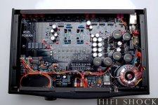
I am not looking for decorated boards. I wanted to know if anyone else could think of times they noticed particularly well-designed boards or board implementation within a component.
Again a PCB may look different to a person without sufficient electronics knowledge but certain sub sections of a pcb will have similar layouts to other pcb's that also have the same sub circuits, the complete pcb's in their entirety may have differing functionalities. As an example, take a switching regulator, the layout onto a pcb will be the same (styles) even if two boards have different functionalities. Read datasheets from semiconductor manufacturers and you'll see preferred circuit layout guidelines.
Any complex electronic device will have a well designed circuit board with the expectation to meet various international standards for emc/emi emissions and there won't likely be much to see from any visual inspection as there will be four or more layers, at best only the top and bottom layers will be visible.
some visual pcb examples would be appreciated.
Of what ?
Schematic and the photograph of the newly proposed twisted differential... | Download Scientific Diagram
If you don't have to be creative anyone could do it.
If you don't have to be creative anyone could do it.
Last edited:
This is a mis-understanding of electronic engineering. You seem to have a fixation with "creativity" and "styles". PCB layouts and engineering may appear to be "creative" to a lay person. A PCB design (complex) will have very deliberate decisions made based upon electrical/electronic circuit theory (preferred techniques) and not because of any sort of "creative flair".
Again a PCB may look different to a person without sufficient electronics knowledge but certain sub sections of a pcb will have similar layouts to other pcb's that also have the same sub circuits, the complete pcb's in their entirety may have differing functionalities. As an example, take a switching regulator, the layout onto a pcb will be the same (styles) even if two boards have different functionalities. Read datasheets from semiconductor manufacturers and you'll see preferred circuit layout guidelines.
Any complex electronic device will have a well designed circuit board with the expectation to meet various international standards for emc/emi emissions and there won't likely be much to see from any visual inspection as there will be four or more layers, at best only the top and bottom layers will be visible.
I think you're too wrapped up in your connotations of the words I'm using. If you look at a bunch of circuits that do the same thing, you'll notice that many of them are different. You can call this difference whatever you want. You can call the mental attributes of the designers whatever you want.
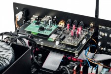
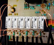
Some examples of interesting solutions:
Here's a Hegel preamp that uses via fencing to shield input traces, which I don't see very often in consumer audio gear.
Goldnote using the same RCA connector as right angle and vertical (you can see the vertical mounted ones on the right).
Lavardin with some fancy pattern on a one-layer board. I think it's decorative, or at least not the ground plane.
Attachments
Functionality of the pcb comes first then prettiness can follow.
If its not functional it doesnt matter how pretty it is it wont work.
If its not functional it doesnt matter how pretty it is it wont work.
Functionality of the pcb comes first then prettiness can follow.
If its not functional it doesnt matter how pretty it is it wont work.
True, I don't think anyone is disagreeing with that. The suggestion that something can be designed to be both optimally functional and aesthetically considered seems to trigger some people.
True, I don't think anyone is disagreeing with that. The suggestion that something can be designed to be both optimally functional and aesthetically considered seems to trigger some people.
Some PC motherboards look amazing, but quite often that's what attracts ordinary Joe Public buyers. They wont appreciate just what technology goes into getting the pcb right for GHz working.
As someone used to drawing designs with pen and ink on paper or mylar (architecture/engineering work) back in the '80s I used to rework published layouts to accommodate available components... usually for friends. Simple stuff.
Since then I have at times dabbled in sketching possible layouts to circuits for which I had no designer PCB layout. No, I don't mean a "Gucci" layout. But I worked at creating ones that respected the circuit and reflected the characteristics of that circuit... symmetry, for instance and keeping traces short to avoid replicating the artifacts of projecting a circuit concept onto a 2-dimensional "drawing". I think there is value in elegance... the PCB layout of a balanced, symmetrical circuit should be symmetrical too. It might even be pretty.
One thing I noticed was that some parts of the circuit would naturally lay out elegantly but the rest wouldn't fit in quite so nicely; that portion tended to a different logic and organization. Eventually it occurred to me to make a break from my pattern of 2-dimensional thinking*. For a Marsh line amp (Pooge Three) I looked into stacking boards and keeping the layouts of each that were elegant on their own separate. This meant that the boards were connected by perpendicular components (chiefly resistors). I figured that there wasn't much difference between a resistor laid against an epoxy board and one standing proud of that board. And it turned out that Marsh's advice about separating signal and power grounds (and ground planes) were implemented inherently. That seemed encouraging.
It was only after playing around with these ideas for a while that I realized that one commercial product, the LYRA CONNOISSEUR 4 Preamplifier, used a similar approach. This "hand-made" complexity might hamper a commercial endeavour but shouldn't hold a hobbyist back.
Admittedly, I've done a lot of sketching and less building. But that has mostly been a matter of circumstance. I've been a committed workaholic and audio has been an oft-neglected hobby. Age and C-19 has changed that somewhat. I hope.
In any event I'm just writing to highlight the possible value of lateral thinking beyond the black box of computer layout generation not necessarily to argue for stacked board designs or to supplant good engineering design practice.
*And to channel Spock. This is supposed to be fun, right?
Last edited:
One thing I noticed was that some parts of the circuit would naturally lay out elegantly but the rest wouldn't fit in quite so nicely; that portion tended to a different logic and organization.
I have written pcb design software.
I quite often use a "swap autoplace" function.
What it does is try swapping two components the same size and if the resulting net is shorter it keeps the change. It does this through the whole pcb.
I can then go in and "fix" star grounding etc.
It can sometimes make the difference between a pcb being routable and unroutable.
If you look at a bunch of circuits that do the same thing, you'll notice that many of them are different.
Nope. To the untrained eye that maybe the case.
Here's a Hegel preamp that uses via fencing to shield input traces, which I don't see very often in consumer audio gear.
That's via stitching, most likely joining two copper planes on different layers together. Used everywhere.......
Last edited:
So what you are saying is that things like loop area or component placement don't make a difference, just connecting the dots is all that is required.
So what you are saying is that things like loop area or component placement don't make a difference, just connecting the dots is all that is required.
I designed a USB scope pcb.
When it arrived I built it up.
If had lovely 10KHz square wave on the signal !
I had run the analogue signal through the middle of a 7660 charge pump and its 10KHz oscillator interfered got picked up nicely.
On another version there was a little 8MHz on the analogue signal.
I had run the analogue signal too close to the microcontroller oscillator circuit.
Once the analogue had been converted to digital I did a low pass filter function on it to kill the 8MHz.
Nope. To the untrained eye that maybe the case.
That's via stitching, most likely joining two copper planes on different layers together. Used everywhere.......
I don't understand your goal. I'm not talking about electrical differences. There is no opinion in "different people do things in different ways."
Please find me more examples of via stitching used in fence-like lines specifically around the input signal traces of an amp. This is the very specific thing I was referring to. I would appreciate it. I actually don't see very many examples of stitching used in hifi analog audio components.
- Home
- Design & Build
- Construction Tips
- PCB Designs to Study