Knocking up a chip-amp power supply PCB and have a quick question - using dual positive regulators (LT1083) with the positive/ground connected (to form quasi-dual voltage), is it better to have pours on both sides of the PCB for + and - and earth traces, or a single pour on the top for just earth and power feeds through (thick) traces?
Cherry told us way back that the power Rails and the power Ground should be adjacent to each other to minimise the effect of radiated interference.
He showed a typical layout implementing this method.
He also applied the same interference rejection to the low level circuits running into and through the PCB.
The ideas and particularly the implementation have not proved popular.
I don't know why, but the vast majority of layout designers completely ignore the need to minimise interference from the power rails.
D.Self did address the issues in his books and on his web pages. But he got it wrong, claiming that separating the power ground made no difference. It was his layout that was wrong rather than the method of reducing LOOP AREA.
Power planes and power ground planes are an excellent way of minimising radiated emi due to the way these minimise LOOP AREA.
Ok, so here are some photos. While I am good with the practical side of things, I am fairly terrible with PCB design (as will be evident).
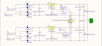
Schematic. Fairly stock standard stuff - however I have a DPDT switch in there between swapping out two resistors (will be wired off board) to change the output level depending on what speaker impedance I am using; I've just thrown some approximate values in so far so these will change depending on what voltage output I'm getting.
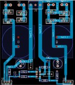
Components and traces. I really struggled to find a 'logical' layout; if they were positive and negative regulators I'd just mirror one side but as they're both positive I couldn't find something that looked ok with both regs in a good position to heat sink. The legs may need to be bent slightly to allow them to clear that trace right on the bottom of the board (which I guess I could move to the component side)
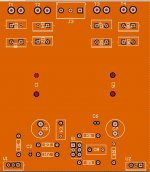
Ground fill. Nothing fancy.
Thoughts/feedback/etc? I'm aware it probably sucks haha

Schematic. Fairly stock standard stuff - however I have a DPDT switch in there between swapping out two resistors (will be wired off board) to change the output level depending on what speaker impedance I am using; I've just thrown some approximate values in so far so these will change depending on what voltage output I'm getting.

Components and traces. I really struggled to find a 'logical' layout; if they were positive and negative regulators I'd just mirror one side but as they're both positive I couldn't find something that looked ok with both regs in a good position to heat sink. The legs may need to be bent slightly to allow them to clear that trace right on the bottom of the board (which I guess I could move to the component side)

Ground fill. Nothing fancy.
Thoughts/feedback/etc? I'm aware it probably sucks haha
Your layout problem starts with the sch.
It is wrong.
pin2 of S1 should read the output voltage at the bottom of C4. Similarly C2 needs to reference that same output node.
Your layout then needs to implement that node. This is where the OUTPUT Zero Volts is.
I think there is comment in the LM317 datasheet that the inductance between 317 out and R1 should be low. This would require R1 to tap onto the 317 Output trace, instead of tapping into the output voltage.
This makes it important that the output +ve node should be kept very close to R1 and 317 out, to minimse the voltage errors that will exist along that trace.
What is C4?
Can't be to stabilise the 317, you have it too far away from the chip.
Because you are using a top side plane, each of the nodes can be a small area of plane and the plane minimises the inductance. Make the plane work for you, you don't need theoretical "point" nodes, close proximity is probably good enough.
Last edited:
Your layout problem starts with the sch.
It is wrong.
pin2 of S1 should read the output voltage at the bottom of C4. Similarly C2 needs to reference that same output node.
Your layout then needs to implement that node. This is where the OUTPUT Zero Volts is.
I think there is comment in the LM317 datasheet that the inductance between 317 out and R1 should be low. This would require R1 to tap onto the 317 Output trace, instead of tapping into the output voltage.
This makes it important that the output +ve node should be kept very close to R1 and 317 out, to minimse the voltage errors that will exist along that trace.
What is C4?
Can't be to stabilise the 317, you have it too far away from the chip.
Because you are using a top side plane, each of the nodes can be a small area of plane and the plane minimises the inductance. Make the plane work for you, you don't need theoretical "point" nodes, close proximity is probably good enough.
C4 is just a bypass cap for C3 - 100uf electro and 0.1uf MKT respectively. C2 is Cadj for the regulator (mentioned in data sheet to improve ripple rejection >60Hz). I need to increase the size as I've just noticed it's the wrong value going through the data sheet (should be 25uf; not 1uf).
Regarding the resistors - I've put a few adjustable regs together before (this is a LT1083, fyi) and I was under the impression that how I've set them up is correct - R1/R4 develop the 1.25v reference voltage and set current, and R2/5 OR 3/6 to the zero-out (also in this case, the -ve rail) via the switch set the output voltage. Pins 2/5 on the switch are connected to the zero-out/-ve too, so as you flick the switch it changed the output voltage dependant on the formula (in the realms of 28 and 32v as listed).
If I have done this somehow wrong, could you please sketch it up quickly as I am struggling to see how your explanation of what I need to change is exactly what I've already done 😕
Cherry told us way back that the power Rails and the power Ground should be adjacent to each other to minimise the effect of radiated interference.
He showed a typical layout implementing this method.
He also applied the same interference rejection to the low level circuits running into and through the PCB.
The ideas and particularly the implementation have not proved popular.
I don't know why, but the vast majority of layout designers completely ignore the need to minimise interference from the power rails.
D.Self did address the issues in his books and on his web pages. But he got it wrong, claiming that separating the power ground made no difference. It was his layout that was wrong rather than the method of reducing LOOP AREA.
Power planes and power ground planes are an excellent way of minimising radiated emi due to the way these minimise LOOP AREA.
I would like to see the Cherry link... I believe what you are on about is Bus bar routing or broadside coupled routing for power and the return....
Why are the majority of PCB designers doing it wrong or are we referencing DIY Audio PCB designers.......
"link" ?I would like to see the Cherry link... ...........
it was in Wireless World before www came into out homes.
Then the only way I had to do any research was to visit the Central Library on George IV bridge and read, read, read.
Ok so I got way better at this. I'm still 99% sure my schematic is correct - can somebody else confirm?
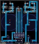
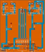
Improvements:
*input/rectified rails are almost symmetrical and running adjacent to each other
*output rails symmetrical and run opposing each other
*'R1' and output caps physically close to regulators
*components almost completely symmetrical
*majority of traces now 1/8"
*0v (incorrectly labeled as GND) has more copper to through-holes
Things to change:
*fix labeling
*remove copper between two input pads for blade connector
I have used power planes (copper pours) in the past.
However now I prefer to just use star grounding.
Its especially important to star ground anything that takes any power like smoothing caps(have strong charging impulses), speaker ground connection and zobel ground connection.
I then connect all audio grounds together that are low current and connect that to the star ground.
He is trying to use 2x Positive regulators. where he needs a Positive and a Negative regulator.
This is perfectly ok. There are two identical, floating supplies connected in series,
with the center connection as common.
No star grounding as has been said in many threads and documents is not the best way, knowing the current loops and controlling them is the best way, and bus bar routing for power gives the cleanest results, noise wise.
"link" ?
it was in Wireless World before www came into out homes.
Then the only way I had to do any research was to visit the Central Library on George IV bridge and read, read, read.
Give us abrief then of what you mean, is it bus bar routing.....
No star grounding as has been said in many threads and documents is not the best way, knowing the current loops and controlling them is the best way, and bus bar routing for power gives the cleanest results, noise wise.
I have designed transistor and valve amplifiers and always had good results with star grounding. The trick is to keep noise out of the low level audio path.
I am referring to the wild spiders legs sort of grounds where signal and return are well separated... separating high current from low current is necessary, keeping noise out of low level signals usually is best done with a ground plane for the low level signals to run next to, careful layout, shielding etc.
- Status
- Not open for further replies.
- Home
- Amplifiers
- Power Supplies
- PCB Design Question