Yes, of course 😆 I am impressed with the punch/dynamic, even if it is sounding a bit 'hot' right off the bench.
So, in another build, physically smaller resistors would be used ...

This is a Miro PCM63 DAC board fueled with bits from a JLsounds I2SoverUSB board.

The thought is to try PCM1704 and TDA1541 with this setup. I had the PCM63 board sitting idle and thought it would be a good start.
So, in another build, physically smaller resistors would be used ...
This is a Miro PCM63 DAC board fueled with bits from a JLsounds I2SoverUSB board.
The thought is to try PCM1704 and TDA1541 with this setup. I had the PCM63 board sitting idle and thought it would be a good start.
of course, that construction was quick'n'dirt iteration, I needed to solve one old but good DAC, unfortunate victim of Audiophool-pockery-tweakery
you know, if I was totally serious, that would be equipped with shunt regs
you know, if I was totally serious, that would be equipped with shunt regs
I have the impression we are not supposed to get TOO serious 😂 This is a case of "lego DAC" to figure out what pleases my ears.
Are you suggesting tweaking the GG shunt to provide +/-30V to the D1, removing/bypassing the onboard PSU?
Are you suggesting tweaking the GG shunt to provide +/-30V to the D1, removing/bypassing the onboard PSU?

Thanks ZM.
Would you know/have an estimate for the current draw of the OS?
For slightly higher gain, in addition to changing R4 (?), would increased voltage rails help?
Would you know/have an estimate for the current draw of the OS?
For slightly higher gain, in addition to changing R4 (?), would increased voltage rails help?
Last edited:
I think came across the answer. Just shy of 40 mA. And change r4 + r11 for a little extra gain.
so current in each first section is neg 30V/string of source resistors
that would be 30V/3K3=9.1mA
buffer Iq is - voltage at gate (30V-(9.1mA*R4 deduct 4V)), divide with 1K5 = 8.2mA
gives sum of, say, 18mA per side
36mA entire shebang
xformer at least 56V center-tapped - try to find adequate close standard one
56Vac * 36mA gives 2VA
so 10VA Donut logical choice ........ of course you can use more
Circa 30V
so current in each first section is neg 30V/string of source resistors
that would be 30V/3K3=9.1mA
buffer Iq is - voltage at gate (30V-(9.1mA*R4 deduct 4V)), divide with 1K5 = 8.2mA
gives sum of, say, 18mA per side
36mA entire shebang
xformer at least 56V center-tapped - try to find adequate close standard one
56Vac * 36mA gives 2VA
so 10VA Donut logical choice ........ of course you can use more
if you increase R4 from 1K5 to 1K8, it'll give you 1.8/1.5 increase of output swing
in any case, don't go above 2K
change R11 downward in value by same ratio; so, if going with R4 to 1K8, change R11 to 1K2 (nearest standard value); that for keeping output source follower current on same level
be sure to check/reset DC level at input node after any change
in any case, don't go above 2K
change R11 downward in value by same ratio; so, if going with R4 to 1K8, change R11 to 1K2 (nearest standard value); that for keeping output source follower current on same level
be sure to check/reset DC level at input node after any change
Last edited:
Encouraged by the "Omni-Enabler", I will try powering the D1 by a 30V Good Gemini shunt.
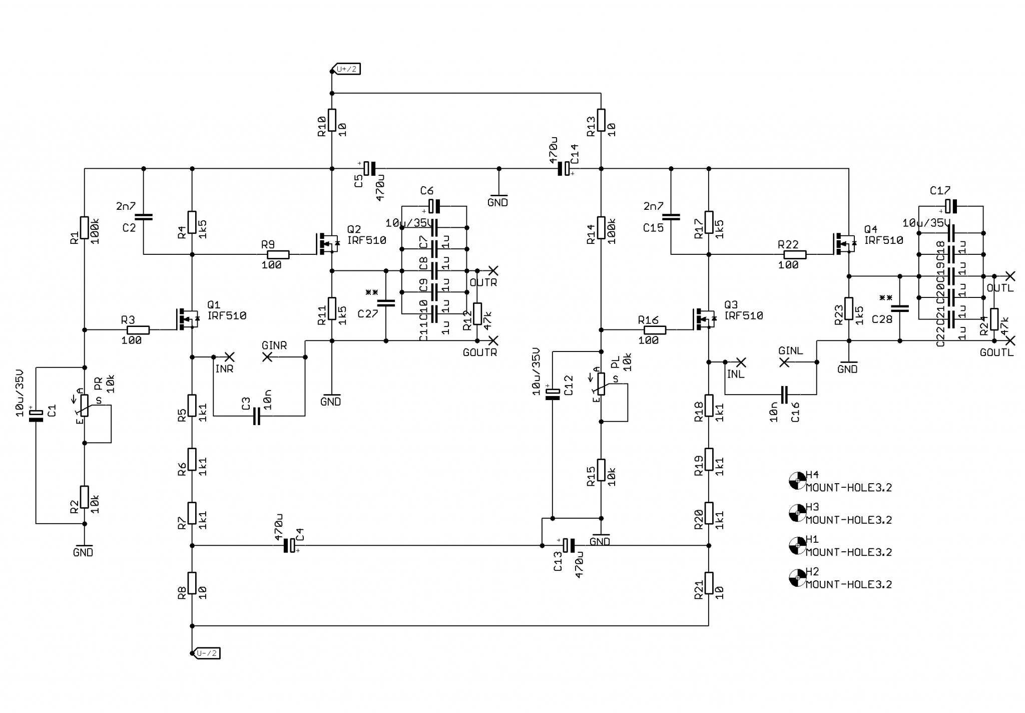
In my naive "lego" approach to electronics, this would work by lifting one leg of R10 and R13 and then feeding +30V there, and similarly feeding -30V to R8 and R21. Does this seem right? (Schematic in previous post). Also, is 10R is what the shunt would ideally like to see?
Cheers
In my naive "lego" approach to electronics, this would work by lifting one leg of R10 and R13 and then feeding +30V there, and similarly feeding -30V to R8 and R21. Does this seem right? (Schematic in previous post). Also, is 10R is what the shunt would ideally like to see?
Cheers
two ways:
- if you're lazy to dismantle existing linear regs, do as you proposed (lifting resistors); of course, disconnect any AC going to local PSUs
- remove (if starting from fresh, do not mount) local PSU, then insert feed from shunts to U+ and U- flags -, say appropriate pins of LM regs
leave 10R resistors in situ; they're there for isolating circuit halves in case of using it as SE Stereo; of course that you can remove 10R resistors and use separate GG regs for each half, having it total mono-block
in that case, take care of programmed current (half of what's needed for entire shebang)
Thanks ZM. Makes sense 🙏
And see, you inadvertently did the enabling thing again... by hinting to the dual mono option 😜
And see, you inadvertently did the enabling thing again... by hinting to the dual mono option 😜
Well. I got the +/-30V shunt connected as suggested, the non-lazy way, but measured 0.75V offset on the D1 input. Turns out, in my excitement I connected the positive shunt wire to the wrong side/hole of the LM317, which must mean I ran D1 on -30V only. Repossitioned the +30 but am now reading 14V offset on D1 input and avout -6V on R10/R13, which really should measure +30V as the input voltage? At least as far my limited understanding goes. Did I fry the mosfets or something else by running it with only the negative rail?
.jpg")
Thanks ZM. You spotted the issue and D1 seems fine. I am a bonehead but glad to report that no Mosfets and DAC ICs were hurt in this episode.
However, Q3 on the GG shunt gets insanely hot, fast, when I dial the A/C voltage above the point where it starts regulating. I can't spot anything obvious, and the bias is programmed to ~71mA. On the negative rail, the raw DC measures -42V on the positive side 35V, suggesting something is amiss causing that voltage drop. It seems to make no difference if disconnected from the D1, suggesting it is a GG construction error. Any suggestions for what to look for/at? I can take this to the GG thread if better.
However, Q3 on the GG shunt gets insanely hot, fast, when I dial the A/C voltage above the point where it starts regulating. I can't spot anything obvious, and the bias is programmed to ~71mA. On the negative rail, the raw DC measures -42V on the positive side 35V, suggesting something is amiss causing that voltage drop. It seems to make no difference if disconnected from the D1, suggesting it is a GG construction error. Any suggestions for what to look for/at? I can take this to the GG thread if better.
Last edited:
GOAT, eh? Did see that one.
So, first clue without unmounting any parts. R2 measures 112R whereas the corresponding R1 on negative rail measures the expected 680R. Color codes of these two resistors are identical though. Guess the corner pasted below would be where to start testing more parts.

So, first clue without unmounting any parts. R2 measures 112R whereas the corresponding R1 on negative rail measures the expected 680R. Color codes of these two resistors are identical though. Guess the corner pasted below would be where to start testing more parts.

Noted. Pulled Q1 and T1 which seem ok. D6 has failed, suggested by measuring, and swapping D6 with with the D5 zener from the other rail reverses the weird resistance previously measured across from R2 to R1, and R2 now measures 680R as expected.
Before proceeding to other end of the faulty rail I wanted to ask if there is any particular reason the zener would give up the spirit, and if it is likely the zener alone quit? It won't be feasible to pull the JFET/SMD2 off for testing...but I may just have to order some fresh parts.
Cheers
Before proceeding to other end of the faulty rail I wanted to ask if there is any particular reason the zener would give up the spirit, and if it is likely the zener alone quit? It won't be feasible to pull the JFET/SMD2 off for testing...but I may just have to order some fresh parts.
Cheers
zener is there to protect JFet from over-voltage
easy enough and enough to check JFet with diode meter - compare with working side (reading few dozens Ohms D to S)
you made some nasty zap along
remember, upping your Mojo is mild while just building by schmts made by other people
where Mojo goes up is when you struggle with problems
either way there is a progress - you'll either solve a problem, or abandon electronics for good
Thanks ZM. As always your input is much appreciated - and I am enjoying the learning curve and am attempting to understand the circuit.
So. Woke up last night thinking about the D5/D6 zeners. They are 20v / 0.5w and should probably be 33v or 30v and >1w? More of a gut feeling than actual insight.
So. Woke up last night thinking about the D5/D6 zeners. They are 20v / 0.5w and should probably be 33v or 30v and >1w? More of a gut feeling than actual insight.
- Home
- Amplifiers
- Pass Labs
- Passlabs D1 (PCM63) vs. Threshold DAC-2 (Ultra Analog D20400a) - who have heard both?