Hello,
I try to build the PassLabs D1 output stage for an PCM1794 DAC. I searched in the old forum threads, but could not find clear answers to my questions... I hope, that someone can help me.
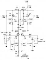
The original circuit is designed for the PCM63 chip, whose current output is +/-2mA. The current output of the PCM1794 is 7.8mA PP. So the output of the D1 in combination with the PCM1794 chip is much to loud. As an solution i would like to reduce the gain of the D1 stage. I read that the gain of this stage is set by the two resistors R27/R34 which are 1K5. To lower the gain i lowered these resistors to 100R, which gives me still to much gain.
So my first question is: how low can I go for R27/R34 without any drawbacks? For example: do i have to change the values of R26/R33 also to avoid that the current through Q3/Q6 is getting higher?
And i found that the resistors R27/R34 form an low pass filter with C15/C16 0.0027uF. This filter has to be recalculated if R27/R34 are changed. If I feed an lowpass-filter-calculator with the values, i find the cut-off frequency at about 40KHz. And vice versa for R27/R34 at 100R, C15/C16 should be 0.04uF to reach cut-off at 40KHz.
My second question: can anyone confirm my calculations?
Thank you for your suggestions and help!
Regards,
Michael

I try to build the PassLabs D1 output stage for an PCM1794 DAC. I searched in the old forum threads, but could not find clear answers to my questions... I hope, that someone can help me.
The original circuit is designed for the PCM63 chip, whose current output is +/-2mA. The current output of the PCM1794 is 7.8mA PP. So the output of the D1 in combination with the PCM1794 chip is much to loud. As an solution i would like to reduce the gain of the D1 stage. I read that the gain of this stage is set by the two resistors R27/R34 which are 1K5. To lower the gain i lowered these resistors to 100R, which gives me still to much gain.
So my first question is: how low can I go for R27/R34 without any drawbacks? For example: do i have to change the values of R26/R33 also to avoid that the current through Q3/Q6 is getting higher?
And i found that the resistors R27/R34 form an low pass filter with C15/C16 0.0027uF. This filter has to be recalculated if R27/R34 are changed. If I feed an lowpass-filter-calculator with the values, i find the cut-off frequency at about 40KHz. And vice versa for R27/R34 at 100R, C15/C16 should be 0.04uF to reach cut-off at 40KHz.
My second question: can anyone confirm my calculations?
Thank you for your suggestions and help!
Regards,
Michael
Attachments
Last edited by a moderator:
Look here.
http://https://www.diyaudio.com/forums/digital-line-level/154866-classic-pass-labs-d1-ess-dac-9.html#post2152628
(Hopefully the link works...)
http://https://www.diyaudio.com/forums/digital-line-level/154866-classic-pass-labs-d1-ess-dac-9.html#post2152628
(Hopefully the link works...)
I read that the gain of this stage is set by the two resistors R27/R34 which are 1K5. To lower the gain i lowered these resistors to 100R, which gives me still to much gain.
So my first question is: how low can I go for R27/R34 without any drawbacks? For example: do i have to change the values of R26/R33 also to avoid that the current through Q3/Q6 is getting higher?
I can't see any drawback to reducing R27/34 as low as you need to go to get the amount of gain that suits you. No need to change R26/33 unless you want to reduce them to run the MOSFETs at higher bias (and hence get more gm).
And i found that the resistors R27/R34 form an low pass filter with C15/C16 0.0027uF. This filter has to be recalculated if R27/R34 are changed. If I feed an lowpass-filter-calculator with the values, i find the cut-off frequency at about 40KHz. And vice versa for R27/R34 at 100R, C15/C16 should be 0.04uF to reach cut-off at 40KHz.
My second question: can anyone confirm my calculations?
They seem fine to me.
Hello Pierre, hello abraxalito,
thanks for your answers. I'm glad, that my thoughts and calculations go in the right direction...
I read the thread of the link you sent me, Pierre. There is one thing i don't understand. What do you mean with: "I could not trim the output voltage to 1.65 V without reducing R24, R31 from 100 K to 68 K." What is this output voltage?
Do I get you right, that if lowering R27/R34 it has only an effect of the gain, not the bias, and that i correct C15/C16 accordingly? That would be easy to accomplish....
And if I would like to increase the bias, i lower the value of R26/R33 and change the C40/C55 values accordingly.
Thank you in advance!
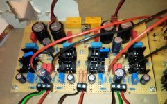
The picture below is the prototype stage in an banana box. Sounds great!
thanks for your answers. I'm glad, that my thoughts and calculations go in the right direction...
I read the thread of the link you sent me, Pierre. There is one thing i don't understand. What do you mean with: "I could not trim the output voltage to 1.65 V without reducing R24, R31 from 100 K to 68 K." What is this output voltage?
Do I get you right, that if lowering R27/R34 it has only an effect of the gain, not the bias, and that i correct C15/C16 accordingly? That would be easy to accomplish....
And if I would like to increase the bias, i lower the value of R26/R33 and change the C40/C55 values accordingly.
Thank you in advance!
The picture below is the prototype stage in an banana box. Sounds great!
Attachments
It was a while ago, but I believe I meant "input voltage" not "output voltage" and 1.65 V is the desired DC voltage of choice for the "output" of that particular ESS DAC.
I believe the rest of your reasoning is correct.
I believe the rest of your reasoning is correct.
And if I would like to increase the bias, i lower the value of R26/R33 and change the C40/C55 values accordingly.
I'm unclear about the role of C40/55 so not sure if they really need changing when the bias is increased. Perhaps 'suck it and see' is the best approach.
If I recall correctly they do form another low pass filter, this one at the input of the I/V concerter. This is in addition to the low pass filter at the output of the I/V. They have different cutoff frequencies. This is simple and elegant.
If you want to throw away some gain, have you considered simply shunting VOL+ and VOL-? You can start with say 500 ohm and adjust from there.
The reason I changed the four resistor values was because the ESS chip outputs four times the current of the PCM63 and this was getting close to the 9 mA bias current going through the MOSFETs in the stock circuit. So I tripled the bias current to be safe.
Last edited:
Yes, I was thinking about putting an resistor or pot between +/- Vol, but didn't like the idea. After some tests and measurements I ended up with 400R for R27/34 and 0.01uF for C15/16. Bias is still in the range of the original construction and the changes do not effect the sounds (as far as i can hear...).
Thank you very much for your help!
Michael
Thank you very much for your help!
Michael

- Home
- Amplifiers
- Pass Labs
- Pass D1 DAC question