Thank you Calvin.
I agree with you there is very little current going through the zeners: 0.3 mA or so. Yesterday I paralleled a 1k resistor with the 1k source resistors R10 and R11 and this changed VcascH and VcascL but only by .03V or so. I need a larger (.2V) change.
I liked your idea of pulling the DC-Servo OPAmp. I removed the chip, and soldered a socket (should have done this to begin with!) and connected Pin 6 temporarily to signal gnd. This made no substantial change. The voltages above and below R5 are about the same, and so is Vriaa. I guess the problem may not be in the DC servo, but is too severe for the DC servo or lack thereof to correct it.
Next… time to play in the buffer and in the regulators for VcascL and VcascH.
Unless mistaken, VcascL is set by D1 and Q98, and VcascH by D2 and Q97, so I could rebuild these with new parts for better symmetry.
Interesting finding. I pulled these components off the pcb and tested them with a lab power supply: R10, Q98, D1, R11, Q97, D2. The regulated voltages that I get (VcascL and VcascH equivalents) are symmetrical within 10 mV. So… these components are well matched to begin with, and the 200mV difference between VcascL and VcascH measured on the pcb is due to a difference in current drawn through R27 and R29 by the positive and negative mirrors. Neither the input, nor the RIAA filter draw enough current to account for the measured difference of 2 mA. This leaves the buffer as a possible cause, or a mismatch between the pos and negative mirrors. If it is the latter, perhaps it can be solved by trimming R19 and R20.
Last edited:
Output buffer
I isolated the buffer by lifting the gate pin of Q99 (2sk170) and connecting it to ground through a 100 ohm resistor.
Although I am no expert, it seems that the buffer current is set by Q91, Q92 and R15 (221 ohm) to slightly less than 8 mA. From my previous J310 curves we know that this current sets Vgs of Q90 (the top J310) to 2.2 V wich sets Vds of Q91 (2sK170) to the same value. I picked a 2sk170 device with Idss slightly above 8 mA so that it runs with Vgs close to zero. I measure Vgs to be +3 mV and hope this is acceptable.
Unfortunately disconnecting the buffer and the DC servo did not remove the asymmetry in the rest of the circuit. So the problem lies elsewhere. Trimming R19 makes no difference: I should have predicted this from the schematic.
Attachments
Last edited:
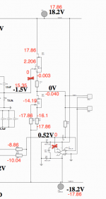
input stage measurements
I am wondering if the input stage is the source of the problem. Does it look like the pnp transistors are matched well enough with the npn transistors?
Thank you Andrew and Calvin for your help so far. I appreciate.
And Happy New Year to all DIYers!
I am wondering if the input stage is the source of the problem. Does it look like the pnp transistors are matched well enough with the npn transistors?
Thank you Andrew and Calvin for your help so far. I appreciate.
And Happy New Year to all DIYers!
Attachments

Last edited:
Hi,
probabely yes.
In my simulation, using BC327-40 and BC337-40 models and without the buffer and DC-servo, the Vriaa settled at ~350mV.
Replacing for example just Q1 by a BC337-25 reduced the offset to ~80mV already.
Also replacing Q30 resulted in a negative offset.
This is as expected if you think about the current distribution in the paradise.
The collector current of Q1 etc. is mirrored into node Vriaaa (current flowing through Q18).
The collector current of Q2 etc. is mirrored also into node Vriaa (current flowing through Q7).
If the current through Q18 is larger than that through Q7 then a positive offset voltage will occur at Vriaa, as the difference current is routed through R9a and R9b towards gnd, creating the voltage drop.
If the current through Q18 is lower than that through Q7 then a negative offset voltage will occur at Vriaa.
After my sim ( I think I used Philips-NXP models) the idle current through Q1 etc. and Q2 etc is roundabout 3.5mA for each transistor.
If You look at the Datasheet from Philips/NXP You will see that the NPN and the PNP show great similarity in the hfe graphs by the value and by the shape of the curves, for all three current classes (suffices -16, -25 and -40).
Especially the graphs for the BC327-25 and BC337-40 are nearly identical in value.
Its very different in the ONSemi datasheet though.
While there is only one hfe graph (-16), the PNP and NPN differ in shape and value.
The PNP is more constant, while the NPN looks a bit sawtooth-ish.
Between 1mA and 10mA the BC337 nearly doubles its hfe.
In other words ... even if You used matched transistors, they could be off-spot, if the matching took place at a different idle current than the working point of the Paradise.
From what the Datasheets say, the Philhips/NXP seem to have clearly greater similarity between the NPNs and PNPs.
You might try as I did in the sim and replace Q1 and following up Q30-Q32 with lower hfe types and see how the Vriaa offset behaves.
From a guts feeling, I´d choose Q91 a SK170 also, matched to Q99 and choose R15=R12.
The offset of the Buffer is very sensitive to idle current variations, reaching dozens of mV, which the dc-servo needs to null-out also.
I´d assume that upper and lower branch will show lower deviations, for example over Temperature, especially when Q91 and Q99 are thermally coupled.
jauu
Calvin
Last edited:
It is my opinion that a DC servoed circuit should be set up to have near zero offset without the help of the servo. Then the servo just has to control the changes that occur during warm up and for weather/temperature variations.
This philosophy requires one to disconnect the servo to get the circuit working inside it's operating window.
If a DC servoed circuit requires an unseen amount of servo correction to bring the controlled parameter to within it's window then a small "other influence" can send the servo hard into it's supply rails.
This can be checked by monitoring the servos output voltage with respect to it's supply rails. If working well within it's operating window then the output should be close to the mid point of the supply rail voltage.
Calvin
This is very useful, thank you!
Most likely, you put your finger on the problem. Indeed I am using ON SEMI BC337-40 NPN devices. HFE was measured using the circuit in post #72, thus at an idle current of 1 mA. As you wrote, the Paradise input stage is flowing between 3.5 and 4 mA through the devices. So the in-circuit HFE of the ON SEMIs might be higher than that of my FAIRCHILD BC327-40 PNPs.
Then Ic in Q18 is 1.6 mA larger than that in Q7. Following your post #3326, 1600 uA times 30 mV translates into a 48 V offset on R9... It is no wonder that the voltage at Vriaa is stuck near Vplus! It all makes sense.
Time to replace Q1 and its neighbours with lower HFE devices.
And I agree with your views on the buffer and will take care of it after fixing the offset. In fact, the plan is to use the famous 'Calvin Buffer' 😀.
Again, thanks for your help. Regards - Pierre
It is my opinion that a DC servoed circuit should be set up to have near zero offset without the help of the servo. Then the servo just has to control the changes that occur during warm up and for weather/temperature variations.
It seems doubtful that Vout can stabilize close to zero without the servo considering the design and gain of this circuit. But I could be wrong...
For the time being I disconnected the servo: OPA chip is removed and the trace of pin 6 is connected to ground.
I will reconnect it once I have managed to reduce the voltage on Vriaa by ANY amount.
I think this is part of your problem.HFE was measured using the circuit in post #72, thus at an idle current of 1 mA. As you wrote, the Paradise input stage is flowing between 3.5 and 4 mA through the devices.
Matching of devices should be done at the operating current.
But, I doubt that an offset as bad as you have, could be due to slight device mismatching.
I suspect another problem.
Pierre just keep going.
I’ve had my Paradise/Calvin build working for over a year now and apart from having an amazingly low noise floor it’s by far the best phono pre that I’ve ever heard.
Sounds just amazing.
You’re almost there.😎
I’ve had my Paradise/Calvin build working for over a year now and apart from having an amazingly low noise floor it’s by far the best phono pre that I’ve ever heard.
Sounds just amazing.
You’re almost there.😎
You might try as I did in the sim and replace Q1 and following up Q30-Q32 with lower hfe types and see how the Vriaa offset behaves.
So… I replaced the Q1, Q30 and Q31 NPNs by lower HFE devices (from HFE 432 to HFE 385-395). This made no noticeable difference to the current drawn. The emitter resistors spread the current evenly between all four devices ncluding Q32 that has a higher HFE.
Next I replaced the NPNs in the current mirror connected to VcascL: Q4, Q5, Q13, and Q14. Again, lower HFE devices made no noticeable change to the currents flowing through the NPNs and PNPs of the input stage.
Last edited:
Some progress
Shoom - Thank you for your kind encouragements. I need them!
At long last… I made some progress. This feels good! 😀
In the current mirror supplied by VcascL, if I reduce R39 from 120 to 103 ohms then the mirror output current flowing through the input stage BC337/NPNs is reduced proportionally. When it becomes close to the current flowing through the input stage BC327/PNPs, then Vriaa gets unstuck and drifts up and down around 2V. This is without the servo.
So it does look like the problem is the mismatch between the BC337 and BC327 devices.
Glad you found a trace towards a solution, sorry I was out due to a bad flu.... but there are lots of experts around here to help, its great to have such a community here!
Agree with AndrewT, the servo is actually very weak, and in the build guide I recommend to check the output voltage of the servo, it should be rather low - a high value indicates mismatch, up to a point where the servo can no longer control it (and that comes pretty quickly...)
Pierre, please keep us posted on the progress and in particular your listening results!
Thanks, will do. First I must order new transistors and do a more exhaustive matching between NPNs and PNPs. I will return here in a while.
Regards - Pierre
Regards - Pierre
Leave the servo disconnected while you debug the circuit.
Once you have the cicuit sorted, then connect the DC servo to control the output offset.
You should see an improvement in the output offset AND see an improvement in output offset drift.
You may not see any improvement in offset "wobble". The servo will probably be too slow to correct for second by second offset changes. But you cannot change the RC constant of the servo (to make it faster) since it will start to correct for the wanted low bass signals and try to remove them as well.
Leave the servo disconnected while you debug the circuit.
Once you have the cicuit sorted, then connect the DC servo to control the output offset.
You should see an improvement in the output offset AND see an improvement in output offset drift.
You may not see any improvement in offset "wobble". The servo will probably be too slow to correct for second by second offset changes. But you cannot change the RC constant of the servo (to make it faster) since it will start to correct for the wanted low bass signals and try to remove them as well.
Disconnect the servo while testing, real good advice and should be done while testing any circuit having a servo. DISCONNECT SERVO WHILE TESTING! 🙂
P.s. Except while testing the servo.
P.s. While the servo is disconnected check if it's output voltage is going to help to solve the offset that you (now) measure at the circuit's output.
P.s. Be sure that the servo has been disconnected at it's output side!
P.s. If the servo is connected to the circuit using a resistor then connect the servo-side of the resistor to ground (while testing).
Last edited:
You were right. That's what I will do. Thank you!Leave the servo disconnected while you debug the circuit.
In the eventuality that my journey may be of use to someone else facing a similar challenge with their Paradise build, I will keep a record of progress in this thread. If it becomes off topic, please let me know.
So, the HFEs of the Fairchild and ON SEMI bipolars in the input stage differ at 4 mA Ic although they were well matched at 1 mA. Going through my bags of devices, the match really is never that great at 4 mA… So it is time to get some different devices, and aim for using the same brand in PNP and NPN positions.
The order includes:
I wish I could find NXPs, for they were supposedly quite nice.
A question: Besides the input stage, where else does matching between PNPs and NPNs matters most? Q49 through Q52? What about Q22 and Q24?
Thank you - Pierre
So, the HFEs of the Fairchild and ON SEMI bipolars in the input stage differ at 4 mA Ic although they were well matched at 1 mA. Going through my bags of devices, the match really is never that great at 4 mA… So it is time to get some different devices, and aim for using the same brand in PNP and NPN positions.
The order includes:
- KSA992FA and KSC1845F as substitutes for BC327 and BC337 (just for the input stage at 4 mA Ic, they would not do well elsewhere where Ic is 15 mA),
- ON SEMI BC327-25, just to see if the -25 devices with the highest HFE will match my ON SEMI BC337-40, and
- DIOTECs BC327-40 and BC337-40.
I wish I could find NXPs, for they were supposedly quite nice.
A question: Besides the input stage, where else does matching between PNPs and NPNs matters most? Q49 through Q52? What about Q22 and Q24?
Thank you - Pierre
Last edited:
Quick question.
I'm building a set of pre regs that are outputting 37v under load (different transformers to cure the noise and they have slightly higher VA). Should I just slug the output of the pre-reg boards with a bigger resistor to drop the voltage. If so what's the optimum voltage?
I figure a 47r should slug me down to near 30v.
Your experience and thoughts please gents.I'll be adding Calvins to the amp boards that these run with if that affects the advice at all, currently the 37v is without Calvins in the middle of things.
Many thanks.
Quick question.
I'm building a set of pre regs that are outputting 37v under load (different transformers to cure the noise and they have slightly higher VA). Should I just slug the output of the pre-reg boards with a bigger resistor to drop the voltage. If so what's the optimum voltage?
I figure a 47r should slug me down to near 30v.
Your experience and thoughts please gents.I'll be adding Calvins to the amp boards that these run with if that affects the advice at all, currently the 37v is without Calvins in the middle of things.
Many thanks.
Mine did the same thing, I dropped it to 26v cause thats what I remember was supposed to sound best. But I cant point to post, maybe someone can confirm.
- Home
- Source & Line
- Analogue Source
- Paradise Builders