Thanks Noted, my comment can be disregarded. Diagram symbol is wrong but otherwise polarity has been flipped in model.No, it's correct, voltage is "-12 V".
Understood why it actually worked now
Last edited:

Another QC design by WhiteDragon with almost same component count but much better in performance.

Cool NanoFarad almost forgot that one.
I believe that thread the OP requested TIP35 specifically.
And also requested a simplified frontend
So it is why lower Ft drivers were chosen. And meet voltage requirements
Of course a more elaborate low distortion design is possible.
But was designed to meet the request of the builder.
For some reason they wanted the gain extremely high, so that could be changed as well.
Very high gain. Gain can be lowered reducing R8 and then R10 be matched to same value.
But yes it shows T4 as VBE for thermal tracking instead of diodes and has simple Zener diode based
current source for Diff.
Again simplified design, to meet request of builder for general purpose transistors.
Good reminder for this thread the 100 ohm degen resistors should be 1% which I noted.
Not specific to either design but specific for any amplifier using Degen in the differential
of course post #42 post looks " upside down" LOL using PNP transistors for input rather than NPN
But if OP for this thread chooses to add a simple current source with zener. This is a example.
Off course values would be adjusted for 12 volt rails not 26 volts.
Last edited:
Yes, i understand. I was the original poster. Anyway is it possible to reduce the gain to around 24dB by raising R18 & without making the amplifier unstable?
Yes correct R18 could be raised to lower the gain.
Stability non issue. Usually people stray away from high resistor values because of possibly noise.
But otherwise because C4 forms highpass filter.
R18 is made to be a higher value so C4 can also be a lower value so it is not so large on the PCB.
Stability non issue. Usually people stray away from high resistor values because of possibly noise.
But otherwise because C4 forms highpass filter.
R18 is made to be a higher value so C4 can also be a lower value so it is not so large on the PCB.
Then instead of raising R18 we can lower the value of R8 & R10 to 22Kohm for 27dB, which is kind of standard gain level (not too high & not too low). Anyway thanks for your replies.
Yes indeed.
Did you build the amp? love to see pictures.
Another fun simple amp. TIP35C use to be available in pretty large packages.
Seen them a lot in MI ( musical instrument) applications.
Low Ft like older 2n3055 but really good gain.
Did you build the amp? love to see pictures.
Another fun simple amp. TIP35C use to be available in pretty large packages.
Seen them a lot in MI ( musical instrument) applications.
Low Ft like older 2n3055 but really good gain.
Unfortunately no, but i promise i'll do it very soon (I'm kinda bored of everything happening in my life) & post pictures for you. I've everything needed for this amp so no problem. But it will be a vero board construction 🙂
What the serpentine line does not tell you: remove the bootstrap C4, and bridge D1, D2, R5 with a large clean-sounding capacitor.No constant current sources (except bootstrap) no vbe multipliers no current mirrrors and no zener diodes.
The circuit is a simplified version of the "audioamp" example circuit in ltspice.
I could probably remove one transistor but the amount of passive components such us trimpots and capacitors would increase significantly,
i should also add an input capacitor and an volume control potentiometer to this circuit.
The reason i chose 2n3055's is becuse i found an literal bag of them (and tesla kd205/203).
Have a good day night or whenever you are reading this post, feel free to leave feedback and suggestions on how to improve this circuit while keeping its simple nature.
View attachment 1372512
View attachment 1372513
And with 2 x 12 volts do use TO-220 as power transes.
He is designing specifically for his collection of T03 transistors.
Which is fine.
The bootstrap or any other constant current source wont even work without a voltage reference.
So no you don't remove the capacitor. It would defy the whole point.
Which is fine.
The bootstrap or any other constant current source wont even work without a voltage reference.
So no you don't remove the capacitor. It would defy the whole point.
geniuenly intrested which transostors would be better kd503/kd502, 2n3055, potentially knockoff bd911's or these things shown in the picture that i only have one pair of?He is designing specifically for his collection of T03 transistors.
Which is fine.
The bootstrap or any other constant current source wont even work without a voltage reference.
So no you don't remove the capacitor. It would defy the whole point.
id increase the supply voltage to 14/15V rails (becuse thats what i would end up with after rectification) increase r2 to 1K to adjust for my parts selection, then make r3 and r17 220m for the same reason and make r1 and r14 an potentiometer.View attachment 1373009
DC analysis with power supply wired correct. All transistors are 22c Temp.
Issues will be listed with quick explanations.
1) VR1 sets differential current at Current meter (AM8) to 6ma. Way to high.
For stability and enough current to drive T3, Typical values would be no more than 1ma to 2ma.
2) Differential transistors current T1 and T2 should be balanced.
Current meters AM4/AM5 show large unbalance 4ma and 2ma.
As expected would result in high DC on amplifier output. VF1 shows
212mV of DC offset. Something acceaptable be no higher than 30mV
and even with simplified circuits would be possible to achieve 3 to 5mV
over a wide temperature range. R2 value is too low and VR1 value should be higher
to set current to 2ma
3) Bootstrap current source R10 and R11 only provides 1.23mA of current for second gain stage T3 shown by current meter AM3
To effectively maintain stable bias current across the diodes. And provide enough AC swing for the whole
amplifier. DC current for T3 to drive T5 and T6 pre drivers and effectively swing to the full 24 volt rails
would need to be at least 6ma. And often in simplified design can be as high as 8ma
R11 and R10 bootstrap resistors should be set lower to achieve at least 6ma of current.
4) pre drivers T5 and T6. Dc current displayed by AM6 and AM7 are not only imbalanced.
At 641uA and 2ma. As emitter follower T5 and CFP T6 to operate as so would require at least
3ma of current. CFP has slight feedback so could likely drive the 2N3055 with less current.
All in All current needs to be higher. R12 and R13 should be set lower for 3ma of current.
5) Power transistors are fortunately not under biased. And surprising Over biased.
At roughly 200ma shown by AM1 and AM2 current meters.
Even though diode string only has 1ma of current. Resistor R5 is too high.
DC bias for quasi class A/B should be around 30ma to 45ma. When the amp has stabilized thermally.
Since we are starting at 22c or roughly cold start. Bias could be as low as 15 to 20ma starting.
And when output transistors get hotter amp will stabilize to 30ma to 45ma.
Since we are at 22c and already high bias. Likely the amp would thermal runaway or get to hot.
Also for more thermal stability R17 and R3 should be higher values than .1 ohms.
.22 to .27 more common. And since thermal tracking with diodes is often debated.
It works fine, but advisable to keep power transistors resistors at higher .27 ohms for thermal
stability and likewise DC stability.
6) R4 is simply not needed and reduces the amplifier bandwidth incredibly low.
Also compensation or Cdom capacitor C2 might need to remain at 100p to stabilize the amplifier.
but would be considered somewhat high. Again often needed to stabilize simplified amplifiers.
without going through a even longer explanation how that value or miller compensation is achieved
and calculated. R9 and R15 degen resistors and C2 would be very effective at stabilizing the amplifier.
and degen might even be raised after amplifier basic DC operating points are fixed. And open loop/closed loop
phase analysis is even possible. R4 lead compensation can be = abandoned
Unfortunately, also transistors were and are not developed according to audio criteria. All that remains is to listen, because even different batches of the same type sound different. They are lucky finds. The easiest way to test the sound of active parts is to insert them into a power supply as a diode - connect collector and basis, then have you got two poles (cb - e = diode). It is this sound that the ear hears. And this sound is the same in all functions of this component, whether as a driver, power, power supply, diode, whatever.geniuenly intrested which transostors would be better kd503/kd502, 2n3055, potentially knockoff bd911's or these things shown in the picture that i only have one pair of?View attachment 1373132
So the ideal is to have an amplifier or other device that runs on a single voltage. For example, a small SE or even a DAC or CD player - many simple, "cheap" ones run with just one voltage - audiophile, exemplary!
2n3055s transistors for 8 w amplifier? Bd439/440 would be enough, or even better a simple tda2030/40/50.
re built it in ltspice and made some "cosmetic" changes to adjust for my parts selectionView attachment 1373068
This is new model with adjusted components, addressing problem list in post #34
DC Analysis shown above^
1) 2) VR1 now sets current at 2ma shown AM8
Differential circuit is as balanced as possible without a mirror roughly 1ma each AM4/AM5
Easily achieved with 1% to 5% resistor R2 910 ohms or E24 to E48 series tolerance resistor.
Differential now balanced shows respectable DC offset at output or VF1 9.77mV
3) Bootstrap current source R11 / R10 changed to 5.5mA
4) Pre Drivers current has been balanced to roughly 4mA and diode added to CFP driver T6
5) Output transistors biased to 30ma set by R5 for better thermal tracking 3 diodes used in the string.
Diodes D1 thru D3 to be mounted close to power transistor heatsink
6) Cdom capacitor C2 lowered to 33p and lead comp resistor removed.
T1/T2 when placed on circuit board should be mounted flat to flat close together for differential thermal matching
Amplifier input AC coupled or DC blocking capacitor C1 added. R1 and C5 form input filter for blocking radio interference.
View attachment 1373074
AC ANALYSIS shown above ^
As noted before, these are expected currents at full clipping 4 ohms
With added diode to T6 CFP driver. AC current between both 2N3055 is now equal AM1/AM2
Unlike before when most AC current went to T8 AM2
Clipping of lower rail symmetrical with no rail sticking. Sorry to lazy to show scope views.
The behavior otherwise well known regardless.
When testing amplifier R5 could be lowered to 33 to 47 ohms to lower bias
and after extended warmup could be raised depending on needed bias.
Model shows 22c for all transistors. Diodes 20c and power transistors 27c for cold start.
Cold start could be set low 10 to 15mA and will reach 30 to 35mA when warm.
I used 30mA in the examples so people dont cry and whine bias is too low
which is why R5 set to a high setting to acheive 30mA at around 22 to 27c
EDIT: i forgot to change to the 2n3055 model
I'm sorry for even using the (wrong) term "RMS power" - apologies!assuming peak power is 21,5V rms power would be more like 15W. (i increased the supply voltage)
For effective sine power you need to use the rms max voltage swing and calculate the power from this value.
thus:
supply = 30 V (assumed value)
max peak voltage swing = +/- 13.5 V peak (supply/2 - 1,5 V)
max rms voltage swing = +/- 13,5 Vpk / sqrt(2) = +/- 9,5 V rms
max effective sine wave power = (9.5 V ^2) / 8 ohm = 11,3 W
alternatively and wrongly you could define the max power using a square wave:
supply = 30 V (assumed value)
max peak voltae swing = +/- 13,5V pk
max effective square wave power = (13,5 V ^2) / 8 ohm = 22,8 W
but, as I said, the latter is not a serious calculation method.
re built it in ltspice and made some "cosmetic" changes to adjust for my parts selection
EDIT: i forgot to change to the 2n3055 model
Cool, we are getting there. Least we have a Quasi output with the diode so its gonna be friendly.
Of course add the 2N3055 for outputs. Since gain and current and what is needed to drive them is
gonna be completely different than shown.
See we are at 14 volts now. VR1 is not constant current but sets the current regardless.
So variation of 12 to 14 volts is going change everything of course.
Using glass type diodes crossed my mind too so 4148 switching diodes be fine.
You can get bias with 2 diodes, but bias will jump like mad once you get it set with right resistor value.
Adjustment will be smoother and easier with 3 diodes.
Better to use 3 diode drops. 68 ohms wont bias the outputs now with 2 diodes.
likely in real life R4 needs to be adjustable. But the model helps you understand
a starting point.
Few issues, were learning. You lowered VR1 so current is going to go up.
Luckily using 3904/06 so they are very easy to drive. Q3 is easy load.
So we never ever need high current for Q1 /Q2.
In fact for stability which we haven't even got to.
Basically simplified, too much current is going to cause stability issues.
Were actually hoping to get to 1ma but 2ma was a tradeoff.
But you raised the current up by changing VR1 to almost 3ma
In order to get T1/ T2 to have equal current for no DC offset.
Were stuck with the limits of R2 and standard resistor values.
You raised it to 1K makes sense, trying to stick to 10% standard values.
But it needed to go down in value, since current was raised up
Anyways, stick to 2ma current for VR1 or were just shooting our own foots.
In fact we can even try to get down to 1ma even. Which will help with stability.
Q3 is easy to drive.
Show you screen shot of new circuit. Kinda went backwards
T1 and T2 not balanced. I'll give you a hint.
You will never ever get it without 5% or 1% resistors
R2 is going to make it happen no way around it.
You can vary R6 in your model or R8 in mine. or the load its driving to help a little.
But its limited to resistor values as well. I made sure to match my resistor numbers
to original model. Cant keep renumbering everything.

Last edited:
Quite a while ago I spent time trying different QC topologies in LTSpice and, IIRC, I got the best THD with the driver resistors / diode connected before the output resistors rather than directly to the output rail, i.e. in the schematic above, R12 to the emitter of T7 and R4/D4 to the collector of T8.
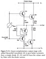
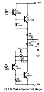
I was intrigued because I've seen at least three versions of the QC topology (see attached): as in your circuit (e.g. D. Self), with just the top resistor directly to the output rail (e.g. B. Cordell) and as described above (e.g. J. L. Hood). The difference wasn't huge and I'm sure it depends on the overall topology, specific transistors used, etc., but you guys may want to give these alternatives a try.
Another thing that seemed to make a big difference was the choice of diode, and this was very dependent on the specific circuit: some times the best was a transdiode (as shown by Self below), sometimes a 1N400x, sometimes something else. Again, worth trying different alternatives.
Attachments
- Home
- Design & Build
- Electronic Design
- Overly simplified quasi complementary amplifier