You need a circuit to invert the input to the lower power device. In the interests of keeping things simple making that a quasi complementary block has been suggested. The added common emitter transistor would invert the input to the lower device.
It would be simpler still to use complementary outputs. The symmetry of FET devices is better than that with bipolar complementary pairs so what advantages are there with a quasi complementary block in those circumstances.
It would be simpler still to use complementary outputs. The symmetry of FET devices is better than that with bipolar complementary pairs so what advantages are there with a quasi complementary block in those circumstances.
You need a circuit to invert the input to the lower power device. In the interests of keeping things simple making that a quasi complementary block has been suggested. The added common emitter transistor would invert the input to the lower device.
It would be simpler still to use complementary outputs. The symmetry of FET devices is better than that with bipolar complementary pairs so what advantages are there with a quasi complementary block in those circumstances.
i dont know firstly i thinked there would be no crossover distortion if no negative fb is used.
Crossover distortion is due to asymmetry of transfer slopes between two output halves. To avoid problems with negative feedback circuits need to be made as linear as possible before application of negative feedback. The transfer slopes should not look like a dog leg. designers thought straightening was possible - at least as far as a distortion meter was concerned. In truth it was like sweeping dirt under the mat.
Hey i found reason to use quasi and the reason is to make a full bridge. ( H bridge )
I think if additional fets are added like in smps and class d there would be a biiig + -> double output voltage and with my +-37 they would be +-70 @ the speakers .. (minus 4v from the IPS)
I dont know if this is invented in audio amps 😀
I think if additional fets are added like in smps and class d there would be a biiig + -> double output voltage and with my +-37 they would be +-70 @ the speakers .. (minus 4v from the IPS)
I dont know if this is invented in audio amps 😀
Used extensively in car-audio. Note, that the load, seen by each half of the bridge, becomes 1/2 of the real load. So, 8 ohm speaker will be seen as 4 ohm. So, each of the bridge halves must be capable of driving 4 ohm speaker then.
Hey i found reason to use quasi and the reason is to make a full bridge. ( H bridge )
I think if additional fets are added like in smps and class d there would be a biiig + -> double output voltage and with my +-37 they would be +-70 @ the speakers .. (minus 4v from the IPS)
I dont know if this is invented in audio amps 😀
If you are convinced of the notion of having identical output device pairing, you might consider using a bipolar quasi complementary output stage.
The symmetry between halves in these is improved if a small signal diode is added in parallel with the emitter resistor connecting the lower PNP driver to the amplifier output. The purpose is to provide and equivalence in the number of diode junctions in the forward conduction path. A small capacitor (22n) in parallel with the diode would make a marginal improvement.
To make a complementary transistor to an NPN - a PNP device requires a different distribution of the N and P doped layers to provide good symmetry between NPN and PNP pairs at low frequencies. The result is better than quasi-complementary pairs in that region, however differences show up at HF where the quasi pair is more symmetric.
As transistor gain declines increasingly at HF added to by stored charge effects in the base regions of output power stages, in the interests of stability loop gain has to be attenuated - rule of thumb - a decade in advance of this declining to one.
There will be much less NFB available at HF than at low frequency.
A contributor on a another thread has highlighted a range of devices made by Semelab specifically for high power audio use - these MG6331 (NPN) a 60 MHz device and MG9411 (PNP) a 35 MHz complement. The manufacturer claims these are superior to the current industry standard devices. Both of these are relatively inexpensive - see
http://products.semelab-tt.com/pdf/bipolar/MG6331 MG6331-R.pdf
http://products.semelab-tt.com/pdf/bipolar/MG9411 MG9411-R.pdf
Of these the NPN device is clearly superior, and in use this type is more robust than PNP complements.
You might investigate a bipolar quasi complementary output stage with MG6331 devices considering the robustness of the device and high power possibilities - before deciding on an all N-Channel bridged arrangement.
HI all, I cant figure out why this is not working 😱
I want to use not a pair, but two equal fets and two temperature compensations.
Definitely commend you for that. If you're gonna use MOSFET finals, either N-Channel or P-Channel: not both in the same circuit. Avoid "complementary" pairs -- and "complementary" MOSFETs are a helluvalot less complimentary than NPN/PNP pairs) means one of two choices: OPT or Circlotron. That OPT-less, complimentary, SEPP topology was originated for BJT finals, and that's what it should be used for. MOSFETs perform poorly when adapted to that topology, but no OPT is cheaper than the cheapest OPT. The Marketing Dept can work to convince you that the "MOSFET sound" (translation: distortion) is the nextest mostest, bestest, kewelestest thing to come down the pike.
What you have here is more appropriate for RF amplification where linearity isn't a big consideration since LC tuners and/or BPFs clean up all the harmonic messes.
Ok all.
I think i know how to implement the H-bridge.
LTP without current mirror (phase splitter), ccs is possible but i dont see reason to use it.
somewhere i readt it is for stopping AC voltage 😀 Its the pair which stop AC and what is this stupidy 😕
Personally I think they are for the Ic's (thermal stability fb).
I see in a lot of circuits use them as a VAS bottom load.
I dont know anything about that. Advantage or not ? Why ?
..
LTP (Ph. split)(with 2xBS170 or 2n7000 -> Two vas-es (with BJTs) -> two biased MOSFET OPS-es -> NFB from A phase to B
dont have patience to test
Last edited:
Ok all.
I think i know how to implement the H-bridge.
...
I talked about complementary pair, not quasi..
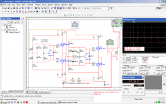
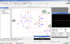
Look @ the example, I simulated two OPS-es and this monster start clipping @ +-73V delivering up to 442W 😱 😱
😱 😱 😱 😱 
Im gonna open thread because this is MONSTER
Attachments
Definitely commend you for that. If you're gonna use MOSFET finals, either N-Channel or P-Channel: not both in the same circuit. Avoid "complementary" pairs -- and "complementary" MOSFETs are a helluvalot less complimentary than NPN/PNP pairs) means one of two choices: OPT or Circlotron. That OPT-less, complimentary, SEPP topology was originated for BJT finals, and that's what it should be used for. MOSFETs perform poorly when adapted to that topology, but no OPT is cheaper than the cheapest OPT. The Marketing Dept can work to convince you that the "MOSFET sound" (translation: distortion) is the nextest mostest, bestest, kewelestest thing to come down the pike.
What you have here is more appropriate for RF amplification where linearity isn't a big consideration since LC tuners and/or BPFs clean up all the harmonic messes.
I gave an explanation of some shortcomings of complementary transistor output pairs at HF where there is less feedback available to correct anomalies due to differences in distribution of N and P layers.
You are now saying that these are more complementary than are MOSFET complementary pairs.
Your explanation of the marketing departments hype using colloquial expressions such as "gonna" and "nextest mostest bestest kewelestest'' are not only trite but untranslatable into other languages.
In plain language what are you talking about and to further serious discussion on this point what source are you relying on as your proof?
I talked about complementary pair, not quasi..
Look @ the example, I simulated two OPS-es and this monster start clipping @ +-73V delivering up to 442W 😱 😱
Im gonna open thread because this is MONSTER
Before you get too committed to this project you should get your current project working properly before moving on. Simulations tell you nothing about component layouts and if you get too far down the track without testing actual hardware you are likely to run into Frankenstein.
Your explanation of the marketing departments hype using colloquial expressions such as "gonna" and "nextest mostest bestest kewelestest'' are not only trite but untranslatable into other languages.
Well, EXCUUUUUUSSSSSEEEE me for writing informally on an informal forum, Mr. Pretentious.
In plain language what are you talking about and to further serious discussion on this point what source are you relying on as your proof?
As for "proof", there is none since proof is a concept relevant to Mathematics only. As for evidence, there is my own personal experience in that every amp that uses these complimentary N-Channel/P-Channel devices in the SEPP topology sounds just plain horrid. They also take out tweeters with all their high frequency garbage.
Even though I don't agree with Douglas Self on everything he says (I disagree with him very much regarding quasi-comp, BJT finals) and I find him overly reliant on measurement. Yes, equipment really can sound better than it measures. (The aforementioned quasi-comp design. Single-ended vacuum triode amps.) He denies this vehemently. That said, I have zero argument with this:
FET versus BJT output stages
On beginning any power amplifier design, one of the first decisions that
must be made is whether to use BJTs or FETs in the output stage. This
decision may of course already have been taken for you by the marketing
department, as the general mood of the marketplace is that if FETs are more
expensive, they must be better. If however, you are lucky enough to have
this crucial decision left to you, then FETs normally disqualify themselves
on the same grounds of price. If the extra cost is not translated into either
better performance and/or a higher sustainable price for the product, then
it appears to be foolish to choose anything other than BJTs.
Power MOSFETS are often hailed as the solution to all amplifier problems,
but they have their own drawbacks, not the least being low transconduc-
tance, poor linearity, and a high ON-resistance that makes output efficiency
mediocre. The high-frequency response may be better, implying that the
second pole P2 of the amplifier response will be higher, allowing the dom-
inant pole P1 be raised with the same stability margin, and so in turn
giving more NFB to reduce distortion. However, we would need this extra
feedback (if it proves available in practice) to correct the worse open-loop
distortion, and even then the overall linearity would almost certainly be
worse. To complicate matters, the compensation cannot necessarily be
lighter because the higher output-resistance makes more likely the lowering
of the output pole by capacitative loading.
(Emphasis mine)
Audio Power Amplifier Design Handbook p. 329
Here, he's discussing the SEPP topology. There's loads more evidence of all the problems caused by using MOSFETs in a design that was originated for very different devices with very different characteristics. If you're using power MOSFETs, then one or the other: P-Channel or N-Channel -- not both -- in the same circuit. The best sonic performance from MOSFETs are designs that use OPTs or the Circlotron topology, or Class A, single-ended, CCS/gyrator/inductor loaded designs.
If you're using power MOSFETs, then one or the other: P-Channel or N-Channel -- not both -- in the same circuit.
I disagree. You just have to treat them right.
Yes - HexFETs "are not designed for audio", having high, non-linear input capacitance. So you have to:
- Drive them with powerful low-impedance drivers.
- Use the optimal value for the gate stoppers.
- Keep the output stage very stable - no sign of any artefacts, like local "ringing".
- Have it properly biased the whole range of working temperatures.
The last point is a very important - often under-valued by designers. Not an easy engineering task by itself.
See this one:
CF-FET V2
Experienced audio engineers, hearing it, can't believe it's got complementary HexFET output stage. It sounds great at all volumes, even at the low ones, without "flattening" the sound. But again - it's not purely because of the way the output stage is organized. Front-end, controlling it - feedback arrangement, voltage gain stages topology - are very important.
- "I don't like cats".
- "You just don't know how to cook them".
😉
Cheers,
Valery
OMG valery non linear input capacitance..
This capacitance doesnt play role at all.
Its even better. One gate stopper and its LPF.
saves you one capacitor 🙂
It only kills, short circuiting RF. much high freq than audible ones
This capacitance doesnt play role at all.
Its even better. One gate stopper and its LPF.
saves you one capacitor 🙂
It only kills, short circuiting RF. much high freq than audible ones
It does matter. Ciss of IRFP240 is 1300pF, IRFP9240 - 1200pF, so one pair gives us 2.5nF.
For 5 pairs (my case), you have 12.5nF. Which is changing non-linearly with Vgd.
Do you want to load your VAS with this capacitance?
I don't.
For 5 pairs (my case), you have 12.5nF. Which is changing non-linearly with Vgd.
Do you want to load your VAS with this capacitance?
I don't.
 Look at it there is no problem 🙄
There is in two cases:
-with the cap referenced to ground (internals are to the reference point like this)
-without R7 and R2, Q5's collector connected to Q8's gate
Everytime there is a way and everytime its the simplest 😉
FET linearity is better and they sound better 🙂
They have high input impedance too, and dont need drivers too.
Attachments
How about you first read something and then make something work for REAL, like bias a MOSFET properly before claiming things that only make you sound more incompetent.
You do understand what 'nonlinear' means? Does your 12nF capacitor simulate nonlinearity? And are you aware that amplifiers don't work only with a single frequency of 1kHz?
my fets are properly biased (thermal compensation is not there of lazines).
i showed capacitive loading, not linearity..
i think this capacitance nonlinearity messes up more HF than 20khz and its no problem. maybe gatedrain capacitance would be a problem.
my fets are properly biased (thermal compensation is not there of lazines).
i showed capacitive loading, not linearity..
i think this capacitance nonlinearity messes up more HF than 20khz and its no problem. maybe gatedrain capacitance would be a problem.
You are suggesting then the internal layout of the chip has no bearing on input capacitance.
- Status
- Not open for further replies.
- Home
- Amplifiers
- Solid State
- output stage with both NPNs