HI all, I cant figure out why this is not working. I want to use not a pair, but two equal fets
and two temperature compensations. Maybe the problem is the simulator ?
Draw a clear schematic diagram from this, and I think you'll see why.
Ohh, second bias voltage must be negative 😀
They must be +-1.25V instead of 2.5v
Another approach is to use bipolar supply..
Or maybe i not know how to bias single polar output stage 😀
They must be +-1.25V instead of 2.5v
Another approach is to use bipolar supply..
Or maybe i not know how to bias single polar output stage 😀
Last edited:
Ohh, second bias voltage must be negative 😀
They must be +-1.25V instead of 2.5v
Another approach is to use bipolar supply..
Or maybe i not know how to bias single polar output stage 😀
this is quite wrong, i lied myself 😀
im too fast..
JUST CANT FIGURE OUT WHY

🙂
i didn't like quasi. my idea is better but cant get it why this is happening 😕
(why to use "inverter" transistor when LTP works as phase splitter too)
Look @ It, It laughts and shows me middle finger.
cant get it, everything is fine at the gates, just even perfect
(why to use "inverter" transistor when LTP works as phase splitter too)
Look @ It, It laughts and shows me middle finger.
cant get it, everything is fine at the gates, just even perfect
Attachments
Last edited:
Your LTP might split the phase but assuming this is a non inverting circuit that function depends on where the inverting input is connected to (0 volts or output?) and any intermediary stages.
i didn't like quasi. my idea is better but cant get it why this is happening 😕
(why to use "inverter" transistor when LTP works as phase splitter too)
Look @ It, It laughts and shows me middle finger.
cant get it, everything is fine at the gates, just even perfect
There's a number of issues in your schematic.
Biasing approach is completely incorrect.
First of all, make sure Vgs is the same for both FETs and you have half of the power supply voltage at the output and, say, 100mA of quiescent current through both of them.
Secondly - you need to make sure, that quiescent current does not grow uncontrolled as the FETs heat up, otherwise, sooner or later, you end up with thermal runaway. Thermal feedback is required for controlling Vgs, mentioned above.
These things will provide you with the right DC operating points. Only after that you can think about driving the FETs from the phase splitter, etc.
BTW, both points are properly addressed in Quasi's designs, but missing completely at your's.
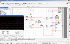
this is for illustrational purposes only !
and everything is fine ofc both voltages are same.
same voltage dividers
and everything is fine ofc both voltages are same.
same voltage dividers
this is for illustrational purposes only !
and everything is fine ofc both voltages are same.
same voltage dividers
No. The way it is shown in post#7 - it will never work.
why ?
u said there must be equal voltages and they are.
thermal fb is another story..
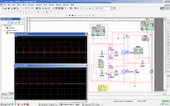
Look @ the gate voltages @ 1st scope.. Max voltage Q1 conducts, Q2 - not, Bias voltage - middle point, Min voltage Q1 not, Q2 conducts ..
u said there must be equal voltages and they are.
thermal fb is another story..
Look @ the gate voltages @ 1st scope.. Max voltage Q1 conducts, Q2 - not, Bias voltage - middle point, Min voltage Q1 not, Q2 conducts ..
Last edited:
OK. It means, you don't understand how transistor works.
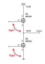
Important thing - reference.
When you want to apply some voltage, it's very important to understand, what it's referenced to. Vgs bias - the Gate voltage, required for linear operation of the MOSFET - must be referenced to its Source.
Q2 - easy. Vgs2 is referenced to Ground.
Q1 - not so easy. It's source is floating together with the output signal. So, you need to arrange the constant Vgs1, assuming that the Q1's Source is floating.
It's not the case in your circuit - both bias dividers are referenced to Ground. That's why it doesn't work.
How are you going to arrange the Q1 bias with the floating reference - that's the question.
I mean - I know a number of good ways how to do it (and can invent a few more if I think a bit). Quasi knows a number of good ways how to do it, but you say you don't like them.
What is your idea?
Attachments
Yes - that's one of the good ways of doing it.
Mosfet54 - note the bias references there!
Just to be precise, I have to note that Japanese design behind Jcarr's link utilizes the Lateral MOSFETs. They don't require thermal feedback, so it is possible to use a simple trim pot for bias setting.
HexFETs (IRF540/9540) do require the thermal feedback. So you need not only setting, but also tracking/regulating it constantly.
HexFETs (IRF540/9540) do require the thermal feedback. So you need not only setting, but also tracking/regulating it constantly.
That load resistor at the end is for the reference. R7
Does not change anything.
Put the probes on your schematic and see the static voltages (with no signal).
Will you see 37V / 2 = 18.5V at the top side of R7?
I guess - you won't.
The whole thing will not work until you see it there.
Does not change anything.
Put the probes on your schematic and see the static voltages (with no signal).
Will you see 37V / 2 = 18.5V at the top side of R7?
I guess - you won't.
The whole thing will not work until you see it there.
ok how half bridge in smps and class d works ?
ok how half bridge in smps and class d works ?
Switching operation is a completely different story. However, this design will not work there either.
Your R3 can't be connected to the ground - this is totally wrong. This way, both Vgs are referenced to the ground. But your top MOSFET's source is much higher. So, the bottom of R3 has to be connected to its source (meaning - to the output). R7 is not required there at all.
Study Japanese schematic more thoroughly - 1k resistors on the left from TR14, TR15 are the same as your R3, R4. See the difference?
- Status
- Not open for further replies.
- Home
- Amplifiers
- Solid State
- output stage with both NPNs