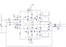
I have a complimentary pair output stage as shown in the schematic. I use the 10K trimmer to adjust the bias. Even though the output is a fixed amplitude sine, typically from rail to rail (or very close), the load varies, even as low as 1R. I let the transistors heat to about 55C, with fan on, and then adjust the bias for 60mA which seems to be the sweet spot where crossover distortion disappears from the scope.
But I have noticed that when the load suddenly is low there is a thermal runaway. I have heatsinks and a fan on the transistors, however I have noticed when the load becomes too low, there is local heat inside the transistors that generates this thermal runaway before it even reaches the outside heatsink. The effect is increased bias, current draw rises until the current limit kicks in. The solution there is to reduce the bias with the trimmer, but this results in crossover distortion when things are "cooler".
So, I am thinking of adding a transistor to act as a heat compensator for the bias, it will have to be mounted on the heatsink of course.
I have all these questions:
1) is it OK to use a transistor mounted on a heatsink for thermal bias compensation? With the long leads leading to this transistor, is it not going to pick up noise and God knows what else?
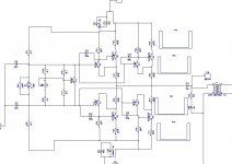
2) I plan to bypass the transistor with an LED/diodes/resistors so that even if we pull the transistor out the max bias will be limited to something small, say, 200mA. This also means that the "range" of the transistor and its "sensitivity" will be less, resulting, I hope in better thermal performance?
3) Is it OK to use a trimmer to adjust the bias of the bias transistor? How will the trimmer perform over time, moisture, heat and so on? Currently there is a single trimmer, and it seems to be OK, except when things get suddenly hot of course.
4) Will the LED generate noise if I use one? I have LEDs from 1.5V to 2.5V, I am thinking of using a 1.88V (red) ? Will the LED be stable in its performance?
I attach "before" and "after" only I have not built the "after" yet.
But I have noticed that when the load suddenly is low there is a thermal runaway. I have heatsinks and a fan on the transistors, however I have noticed when the load becomes too low, there is local heat inside the transistors that generates this thermal runaway before it even reaches the outside heatsink. The effect is increased bias, current draw rises until the current limit kicks in. The solution there is to reduce the bias with the trimmer, but this results in crossover distortion when things are "cooler".
So, I am thinking of adding a transistor to act as a heat compensator for the bias, it will have to be mounted on the heatsink of course.
I have all these questions:
1) is it OK to use a transistor mounted on a heatsink for thermal bias compensation? With the long leads leading to this transistor, is it not going to pick up noise and God knows what else?
2) I plan to bypass the transistor with an LED/diodes/resistors so that even if we pull the transistor out the max bias will be limited to something small, say, 200mA. This also means that the "range" of the transistor and its "sensitivity" will be less, resulting, I hope in better thermal performance?
3) Is it OK to use a trimmer to adjust the bias of the bias transistor? How will the trimmer perform over time, moisture, heat and so on? Currently there is a single trimmer, and it seems to be OK, except when things get suddenly hot of course.
4) Will the LED generate noise if I use one? I have LEDs from 1.5V to 2.5V, I am thinking of using a 1.88V (red) ? Will the LED be stable in its performance?
I attach "before" and "after" only I have not built the "after" yet.
Attachments
Cordell gave an explanation of Thermal instability in BJT & Vertical mosFET output stages.
He also gave a method for determining the minimum emitter/source resistor required.
This value depended on transistor gain, transistor interface resistance and supply voltage.
It was if I recall correctly in his "interview" series, possibly the output stage Thread.
He also gave a method for determining the minimum emitter/source resistor required.
This value depended on transistor gain, transistor interface resistance and supply voltage.
It was if I recall correctly in his "interview" series, possibly the output stage Thread.
You have a transistor marked D14, that must be thermally connected to the output heat sink for stabilization. Output transistors warm up, their gain increases and the current increases D14 warms up and the gain increases so the C E voltage reduces and reduces the Bias voltage to compensate the output transistors and stops thermal runnaway.
I have built it and tested it. Bias control transistor mounted on heatsink very close to one output transistor.
The bias transistor fails to control the thermal runaway, it does not respond as fast and as widely as would be needed. The reason is two fold. First, the thermal runaway is almost instant as soon as the load is applied, the heat rises inside the output transistors and does not reach the heatsink in time to affect the bias transistor. Secondly there are about 5-10C difference between heatsink and bottom of output transistor case. Thirdly the temperature change on the bias transistor, from say 25C to 50C takes a while to happen, while the output transistors are already at 70C, and even when the temperatures have settled, the resulting bias is unacceptably high. Reducing the bias at 70C results in a lot of crossover distortion at 25C.
It appears this circuit is no better than the simple diode providing bias. On the simulation things are quite different, and appear to work just fine 🙂
I suspect your bias setting is far too high if the transistors cook straight away.
In my designs I have found I could get away with 10-20mA bias current. Measured across source/emitter resistor.
I am told Peavey also believe in minimal bias currents in their designs too.
So long as you have sufficient bias current to kill crossover distortion it should be fine.
Any more is just lost in heat with little benefit.
Your driver into the output transistors is inverting with gain.
This will make your bias setting very touchy.
I would change the driver to none inverting system and see if that improves things.
I found setting the bias was a little touchy even with no gain.
This will make your bias setting very touchy.
I would change the driver to none inverting system and see if that improves things.
I found setting the bias was a little touchy even with no gain.
Your output stage is CFP.
I can not read from your circuit what driver transistors you have used?
You need to monitor the drivers, not the output transistors.
Thermally connect your VBE-multiplier to these driver transistors only.
Or; omit the VBE-multiplier (and your bias led) complitely and make two "diodes" out of the same type transistors (npn and pnp) as your drivers and connect these "diodes" in series. Then put these "diodes" and all 4 driver transistors under the same heatsink on your PCB.
I had very VERY! good results that way, with absolute ZERO crossover distortion.
Here is 100kHz 1W from an amplifier made that way...

Red input, blue output.
I can not read from your circuit what driver transistors you have used?
You need to monitor the drivers, not the output transistors.
Thermally connect your VBE-multiplier to these driver transistors only.
Or; omit the VBE-multiplier (and your bias led) complitely and make two "diodes" out of the same type transistors (npn and pnp) as your drivers and connect these "diodes" in series. Then put these "diodes" and all 4 driver transistors under the same heatsink on your PCB.
I had very VERY! good results that way, with absolute ZERO crossover distortion.
Here is 100kHz 1W from an amplifier made that way...
Red input, blue output.
Last edited:
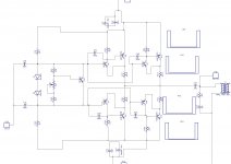
I hope the schematic is easier to read now.
The previous version was using two diodes. Nothing thermally attached to anything. The current setting adds a bias transistor thermally attached to the output transistors.
The bias is set at around 50C, on no load, until the crossover distortion disappears from the scope. This is around 30mA per output transistor pair (60mA in total).
The bias is stable using just two diodes and a trimmer bypassing one of the diodes. Except for the below condition:
Until the load decreases to about 1R, and the amplitude exceeds a certain level (typically just over 16V p2p). That combination causes an instantaneous thermal runaway. If the amplitude was a bit less, say 15.5V p2p, then there are no problems at all.
To "fix" this thermal runaway I can
(a) decrease the bias - but then I get crossover distortion at lower levels of drive/load
(b) increase the supply rails to a minimum of about 3.8V over from the peak of the curve - the problem disappears. But as this is a battery operated device I cannot simply afford all those extra volts on the rails.
(c) add a bias transistor to the simple diode arrangement as shown in this schematic. Unfortunately this does not offer an improvement over the diodes.
I will try more of your suggestions and see what happens.
Attachments
![output_stage_bias_3[1].jpg](/community/data/attachments/386/386960-6accd6ab14966cc40797228af3f12da9.jpg?hash=aszWqxSWbM)
The problem is that the drivers are TO-92 devices, and unless you cook them there will be practically 0 temperature difference on the heatsink, on any heatsink. In practice those BC327/BC337 drivers run at 2C-5C above ambient and without heatsinks, while the output transistors are cooking and on a heatsink and a fan.
Maybe if I change the driver transistors to something more beefy, for example MJE243/253 then those may provide better thermal stability.
Maybe if I change the driver transistors to something more beefy, for example MJE243/253 then those may provide better thermal stability.
Just to maintain my sanity I just tried a LM3886 (a power amp made by NS), it also CANNOT deliver 8V peak into 1R load with anything less than +/- 14-16V rails. So it seems my power stage is actually better because it can do it with about +/- 12.5V rails. The LM3886 also gets mightly hot even though mounted on a huge heatsink.
Edit: actually the LM3886 can approach the positive rail much better than the negative rail, at high loads, for 8V peak into 1R it requires +12.5V / -14.5V minimum.
Edit: actually the LM3886 can approach the positive rail much better than the negative rail, at high loads, for 8V peak into 1R it requires +12.5V / -14.5V minimum.
Last edited:
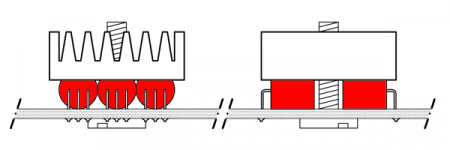
could use this... for example...
and if you wrap the transistors in copper foil (tape), even better...
and if you wrap the transistors in copper foil (tape), even better...
Attachments
Last edited:
Cordell gave an explanation of Thermal instability in BJT & Vertical mosFET output stages.
He also gave a method for determining the minimum emitter/source resistor required.
This value depended on transistor gain, transistor interface resistance and supply voltage.
It was if I recall correctly in his "interview" series, possibly the output stage Thread.
I did a search for "cordell" and "thermal" but did not come up with anything, would you have a link please?
searched bob cordell and thermal stability and found
http://www.diyaudio.com/forums/soli...l-interview-bjt-vs-mosfet-60.html#post2052523
There are other posts. It applies to both mosFETs and BJTs.
http://www.diyaudio.com/forums/soli...l-interview-bjt-vs-mosfet-60.html#post2052523
There are other posts. It applies to both mosFETs and BJTs.
akis, I have never seen a power amp like this. what are the rail voltages, how much power are you trying to get in 1R? how much gain does this amp have, closed loop? do you have a schematic that shows the entire amp design excluding the power supply?I have a complimentary pair output stage as shown in the schematic. I use the 10K trimmer to adjust the bias. Even though the output is a fixed amplitude sine, typically from rail to rail (or very close), the load varies, even as low as 1R. I let the transistors heat to about 55C, with fan on, and then adjust the bias for 60mA which seems to be the sweet spot where crossover distortion disappears from the scope.
But I have noticed that when the load suddenly is low there is a thermal runaway. I have heatsinks and a fan on the transistors, however I have noticed when the load becomes too low, there is local heat inside the transistors that generates this thermal runaway before it even reaches the outside heatsink. The effect is increased bias, current draw rises until the current limit kicks in. The solution there is to reduce the bias with the trimmer, but this results in crossover distortion when things are "cooler".
So, I am thinking of adding a transistor to act as a heat compensator for the bias, it will have to be mounted on the heatsink of course.
I have all these questions:
1) is it OK to use a transistor mounted on a heatsink for thermal bias compensation? With the long leads leading to this transistor, is it not going to pick up noise and God knows what else?
2) I plan to bypass the transistor with an LED/diodes/resistors so that even if we pull the transistor out the max bias will be limited to something small, say, 200mA. This also means that the "range" of the transistor and its "sensitivity" will be less, resulting, I hope in better thermal performance?
3) Is it OK to use a trimmer to adjust the bias of the bias transistor? How will the trimmer perform over time, moisture, heat and so on? Currently there is a single trimmer, and it seems to be OK, except when things get suddenly hot of course.
4) Will the LED generate noise if I use one? I have LEDs from 1.5V to 2.5V, I am thinking of using a 1.88V (red) ? Will the LED be stable in its performance?
I attach "before" and "after" only I have not built the "after" yet.
Last edited:
It is not an audio amp, but very similar anyway. The specs are 7V-8V peak into 1R-1.5R. About 16-30 watts on the load. Rails are 10.6V to 13V each side. There is no gain, it is a current buffer.
Having tested earlier on a LM3886, I discovered it also cannot approach the rails based on the above specs. However the schematic above manages to at least produce an almost perfect sine out of about 12V-12.5V rails, whereas the LM3886 needs at least -14.5V on the Vee rail. So in this respect mine is better 🙂
Having tested earlier on a LM3886, I discovered it also cannot approach the rails based on the above specs. However the schematic above manages to at least produce an almost perfect sine out of about 12V-12.5V rails, whereas the LM3886 needs at least -14.5V on the Vee rail. So in this respect mine is better 🙂
akis, i don't know what kind of amp this is but the bias transistor or (VBE Multiplier) must be mounted on the heat sink as you have said you've done. Using a trimmer pot to set the bias is ok if it is sealed. the only suggestion i have is to replace the bias transistor with an mpsa14. this is a darlington transistor and has a gain of 5000 @ 10ma. it will react quicker thermally.It is not an audio amp, but very similar anyway. The specs are 7V-8V peak into 1R-1.5R. About 16-30 watts on the load. Rails are 10.6V to 13V each side. There is no gain, it is a current buffer.
Having tested earlier on a LM3886, I discovered it also cannot approach the rails based on the above specs. However the schematic above manages to at least produce an almost perfect sine out of about 12V-12.5V rails, whereas the LM3886 needs at least -14.5V on the Vee rail. So in this respect mine is better 🙂
searched bob cordell and thermal stability and found
http://www.diyaudio.com/forums/soli...l-interview-bjt-vs-mosfet-60.html#post2052523
There are other posts. It applies to both mosFETs and BJTs.
Dear God, this is 300+ pages! I read the last pahges and now reading fromt he start. Back to 2006.
I believe the summary is like "use 0.27R emitter resistors" but one needs to consider the final load. At 8R you may be able to use 0.27R, maybe two parallel transistors to reduce to 0.135R in total, representing 1.69% of the load. But when the load drops to 1R, then we are at 13.5% of the load, which is an unacceptable power loss.
One way to go around this may be to keep the 0.27R and add more parallel transistors, so instead of 2 transistors with 0.1R emitter resistors, have 5 transistors with 0.27R resistors.
I am running some simulations to work out the power distribution etc.
- Status
- Not open for further replies.
- Home
- Amplifiers
- Solid State
- output stage thermal stabilisation