I have been working on a power output design, delivering around 25W @ 180-220KHz on the load, that has been working for over 6 months now. It is simple push-pull, 3 complimentary pairs on each side, making a total of 3+3 drivers and 3+3 output transistors. I have a 100pF B-C capacitor on every driver and that seemed to stabilise the system.
The original design was powered by +/-12V and the transistors were BC327/BC337 for drivers and MJE150xx for outputs.
Then I changed the power supply to +/-24V and could not use the BC327/BC337 any longer (low Vce). After some experiments I used the ZTX653/ZTX753 as drivers (they are tiny, even smaller than the BC327).
I decided to be adventurous and try "improving" on the MJE150xx output transistors and so I tried the D44H11 and D45H11. Using them I got lots of oscillations so I quickly reverted back to the MJE150xx and this worked with no issues and have been using it since.
A few days ago I decided to make a "copy" in case the current working one breaks, and yes I decided to be adventurous again and used the D44H11/D45H11.
I once again got the oscillations (under moderate load). But this time I decided to investigate. So I have read all about base stoppers and so on. But then I realised an important fact that I would like your help with. It seems the oscillations are a multiple or some product of the input frequency. For example at 200KHz the oscillations appeared to be at 8MHz. At 2KHz they were quite low, in the audible range maybe (my dummy load resistor and its heatsink act as an audible resonator).
From what I have read about output stage oscillations they are unrelated to the input signal's frequency. Or are they? What should I do next to investigate this further?
An interesting possibility
If you're using a digital scope for the measurements, you can sometimes be fooled by aliasing, depending upon the sampling rate...so there's a possibility that what you're seeing might (or might not) be real.
If you're using a digital scope for the measurements, you can sometimes be fooled by aliasing, depending upon the sampling rate...so there's a possibility that what you're seeing might (or might not) be real.
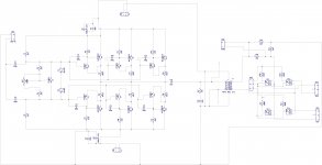
Simulation works well. Except thermal runaway. Here is a schematic, showing the MJE150xx instead of the problematic KSE44H11 and KSE45H11.
Do I need base stoppers? Where should they be placed? How would I calculate the right value? If not base stoppers what else could be causing these oscillations (under load only). Square waves are also problematic (not that I need them, but just saying).
Do I need base stoppers? Where should they be placed? How would I calculate the right value? If not base stoppers what else could be causing these oscillations (under load only). Square waves are also problematic (not that I need them, but just saying).
Attachments
Yes, base stop helps. 2.2 ohm might work. Square wave is for showing the overshoot and ringing. If you have ringing and over shoot, that means the phase margin is not enough.
If simulation looks much better than the real circuit, then you might have layout problem.
If simulation looks much better than the real circuit, then you might have layout problem.
The main problem is the improper use of the resistors: R7, R8, R11, R12, R15, R16. If you want to eliminate output stage oscillations, you will have to move these resistors in the emitter transistors: Q4, Q5, Q8, Q9, Q12, Q13. So, try this move.
Yes, base stop helps. 2.2 ohm might work. Square wave is for showing the overshoot and ringing. If you have ringing and over shoot, that means the phase margin is not enough.
If simulation looks much better than the real circuit, then you might have layout problem.
If that's the complete circuit, it's unity gain with no feedback so it oscillating is a bit strange. Mind you, the output transformer is a 4:1 step-up so there could be layout problems with the secondary feeding back to the input at RF.
My guess it's either CFP instability or parasitic/layout problem. But he did say it follow the input frequency. So I am not sure.If that's the complete circuit, it's unity gain with no feedback so it oscillating is a bit strange. Mind you, the output transformer is a 4:1 step-up so there could be layout problems with the secondary feeding back to the input at RF.
I was only meaning to show up to the output capacitor, but somehow the whole circuit got printed.
On the test circuit there is no transformer, I am testing at the output capacitor.
Regarding the emitter resistors, I thought the compound pair's emitter is the first transistor's emitter.
These oscillations (under load) do not happen when the output transistors are MJE150xx but happen with faster transistors such as KSED44H11/D45H11.
The PCB is exactly the same as the one that works happily with the MJEs.
It would appear that the oscillations, which result in all sorts of trouble, are some function of the input signal, some multiple maybe. Certainly at 200KHz input, I could clearly see the main wave modulated by a much faster wave, and when I tuned the scope on to it it was like 8.5MHz. With low input frequencies, such as 5KHz, the oscillations were much lower (but I did not measure).
If base stoppers have been known for ever to cure such problems, could you please tell me exactly where I need to place them? I might start hacking the PCB to see if it will provide stability.
I'm with donpetru, the emitter resistors should be on the MJEs. There the emitters with most of the current. Not sure it will help the oscillation but it will help with the current sharing.
Yes, emitter resistor is absolutely necessary. Not just current sharing, more important, it reduce the gain of the local loop as you can look at it as common emitter stage. Having degeneration reduce the gain and MAYBE stabilize the stage.
But I would at least try to put beats on the base lead if OP does not want to butcher the board.
I have a thread on trying to get rid of the base stop resistor as I did simulation that the base stop resistor cause voltage drop because of base current that is non linear due to high current beta droop. I just wonder whether ferrite beats can do the job.
May I ask if you are absolutely certain that the degenerative emitter resistors should be connected to the emitters of the second transistor of the Sziklai pair and not the first? It is common emitter stage, but it is the first transistor which is common emitter, the second transistor is a bypass. That is how I understand it anyway. Am I wrong?
Where would you suggest this base stopper goes? Base of the first transistor or base of the second transistor in the pair?
Where would you suggest this base stopper goes? Base of the first transistor or base of the second transistor in the pair?
Hi Akis,
The same example I just mentioned in the other thread - working in real life stable dual-CFP output stage - well, this one employs Hex-FETs at the output, but the principle is the same as for BJTs, just the stoppers R value will be lower.
>CFA-CFPx2 high-performance amplifier<
It works at relatively low quiescent current and sounds excellent even at low volume.
Cheers,
Valery
Valery,
It seems you have a compound pair composed of a BJT bypassed by a MOSFET. The pair acts as a BJT whose pin outs follow the first transistor's, so that your emitter degenerative resistors are placed just like mine.
There are base stopper resistors, 220R into the gate of the MOSFET.
We know that BJTs get stuck in saturation and find it hard to switch off. This lag means that within a compound pair, the second BJT lags behind, causing it to remain open much longer than it should (out of time), overlapping the other side which has also opened (in time) and creating cross-conduction, which is terrible as it leads to thermal runaway.
This cross-conduction is much more evident at high frequencies because it is there where the "slowness" of the second BJT within the compund pair comes into play.
In my case the normal operating frequency is 200KHz. Therefore I have used low collector resistors, 33R, to allow the driver BJT to be able to draw the excess charge off of the base of the power BJT quickly enough to eliminate cross conduction.
But now we are placing a resistor in series to the base, which is counter intuitive, the exact opposite of what we are trying to achieve with eliminating cross conduction.
I shall go place these resistors now, I am just wondering if by doing this I will be opening myself to cross-conduction issues.
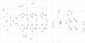
Placed 1R5 base stopper resistors with no change. Placed 3R0 resistors slightly better but still not there.
The 3R0 resistors are almost 1/10 of the collector resistors (33R). Should I increase them further, I will be severely impacting on the purpose of the 33R collector resistors (low enough to allow the base charge to drain quickly so the BJT can switch off quick).
But I will try 10R to see what happens.
I'm with Alan and donpetru. Degenerate the driver transistors and you will see the stage behave in a more stable manner. This is one trick that the majority of CFP users miss...
I placed 10R resistors and that has almost fixed the problem, except a small kink on the negative side that does not go away with increasing bias. I will have to try higher values still, maybe 15R or 20R.
How do I degenerate the drivers?
How do I degenerate the drivers?
OK! Success! I have used 15R base stopper resistors and to compensate I lowered the collector resistors to 22R - it works perfectly and no issues , except the drivers now get a little bit hotter (we are using the drivers more than before).
I attach the schematic that works.
Two questions remain:
1) is it better to use slower/different transistors that work without base stoppers
2) is it better to use faster transistors but now be obliged to use base stoppers and drive the drivers harder than before?
I attach the schematic that works.
Two questions remain:
1) is it better to use slower/different transistors that work without base stoppers
2) is it better to use faster transistors but now be obliged to use base stoppers and drive the drivers harder than before?
Attachments
I think you are right,.............Regarding the emitter resistors, I thought the compound pair's emitter is the first transistor's emitter...............
the driver has an emitter resistor. This passes current from the driver and the output. The driver current is near constant, so the emitter resistor is effectively monitoring the output device current.
Each driver is dedicated to it's output device. So it's the driver's emitter resistor that rules.
- Status
- Not open for further replies.
- Home
- Amplifiers
- Solid State
- Output stage oscillations