Hello everyone!
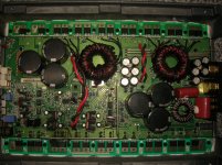
Again here, with this old amplifier ...
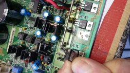
Well, nothing open, I have encountered this "MOD" which is new to me.
my question is:
Should I remove this mod, capacitor, bridge and replacing resistor R40 before starting measurements?
Again here, with this old amplifier ...
Well, nothing open, I have encountered this "MOD" which is new to me.
my question is:
Should I remove this mod, capacitor, bridge and replacing resistor R40 before starting measurements?
Attachments
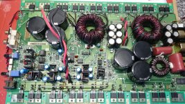
The cap and jumper are factory suggested mods.
I can't tell what they did with R40 so I can't make any suggestion about that. They typically made mods to that part of the circuit to disable the over-current protection circuit.
I can't tell what they did with R40 so I can't make any suggestion about that. They typically made mods to that part of the circuit to disable the over-current protection circuit.
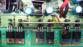
From your pics it looks like you have some audio outputs to replace along with driver ic too for starters.
I understand what the "mod" factory ... but I'm not sure, to leave it as is, or remove the IC ..
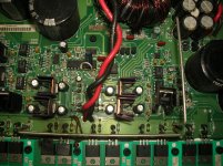
I have found that the R40 had been replaced by a normal resitor, 1/4 watt,, (go technicians .. !!)
And yes, the eight audio output MOSFET are burned, and the resistor of the gate of one of them, increased their value.
I have found that the R40 had been replaced by a normal resitor, 1/4 watt,, (go technicians .. !!)
And yes, the eight audio output MOSFET are burned, and the resistor of the gate of one of them, increased their value.
There isn't likely anything wrong with the 3526 so there's no reason to remove the modification with the jumper and capacitor.
The other modification was likely to disable the over-current protection, especially if the end of the resistor that would have connected to the shunt resistors was connected directly to ground. With the over-current disabled, it's much more likely to destroy the power supply when the output FETs fail. If the owner wants the over-current protection disabled, you need to determine if you're going to cover it under warranty. I would not let it go with the over-current protection disabled.
The other modification was likely to disable the over-current protection, especially if the end of the resistor that would have connected to the shunt resistors was connected directly to ground. With the over-current disabled, it's much more likely to destroy the power supply when the output FETs fail. If the owner wants the over-current protection disabled, you need to determine if you're going to cover it under warranty. I would not let it go with the over-current protection disabled.
Well, it seems that this amplifier is giving a little war ...
Replaced parts: U9 U10 and U17, Q101, Q102, Q103, Q12, Q26, Q107, Q108 and Q109.
When connected, protection LED lights two seconds, and two seconds, Q12 exploited, and all other FETs that part are shorted.
I extracted all fet that area.
And I made some measurements:
U14:
pin 1: 5,02
pin 2: 3,9
pin 3: 4,24
pin 4: 4,69
pin 5: 4,55
pin 6: 0
pin 7: 0
pin 8: 4,55
pin 9: 3,7
pin 10: 1,74
pin 11: 0
pin 12: 4,72
pin 13: 6,88
pin 14: 16,10
pin 15: 0
pin 16: 6,9
pin 17: 16,14
pin 18: 5,02
U17
pin1: 0
pin2: 0
pin3: 0
pin4: -9,8
pin5: 0
pin6: 4,5
pin7: 9,9
pin8: 0,14
U9
pin1: 0
pin2: 4,0
pin3: 2,8
pin4: 0
pin5: -10,4
pin6: -3,1
pin7: -10,3
pin8: 9,2
(pin 2 and pin3 before this measurement result, negative values were becoming..)
I've been looking at previous post about this amp, but I get not find anything clear ..
what do you think, Perry?
Desolder the red/black wires (after discharging the caps). Desolder from the rectifier side of the board.
Now you can power up the amp and check all drive signals on the outputs without risking any damage to the outputs. You will to jump pins 2 and 6 of U17. You may also have to connect the source leg of Q101 to the negative speaker terminal.
Now you can power up the amp and check all drive signals on the outputs without risking any damage to the outputs. You will to jump pins 2 and 6 of U17. You may also have to connect the source leg of Q101 to the negative speaker terminal.
It seems that I have not been lucky, "I screwed up" (as they say vulgarly ..)
I disconnected two cables voltage rail, (but I have not disconnected the other two ..) as you Perry said.
I connected the amplifier, and new Q12 has issued a flash, this time from behind the motherboard.
I measured these FETs continuity and curiously does not appear no short ...
I have to ask more pieces ...
Attachments
Well, I have new measures...
Pin 2 and pin 6 of U11, linked by a cable, and also have connected the source leg of Q101 to the negative speaker terminal.
And these are the results:
U14: same measures in the post #7
U11
pin1: 0
pin2: 0
pin3: 0
pin4: -9,78
pin5: 0
pin6: 0
pin7: -0,12
pin8: 9,98
U17
pin1: 0
pin2: 0
pin3: 0
pin4: -9,7
pin5: 0
pin6: -0,3
pin7: 9,99
pin8: 1,1
U9
pin1: -0,03
pin2: 0,3
pin3: -0,03
pin4: 0
pin5: -9,8
pin6: -6,58
pin7: -9,5
pin8: 9,9
U8
pin1: -9,6
pin2: 0,3
pin3: -0,1
pin4: -9,7
pin5: -0,3
pin6: 0,2
pin7: 9,9
pin8: -9,6
U7
pin1: -9,2
pin2: 0
pin3: 0
pin4: -9,7
pin5: -0,07
pin6: 0,4
pin7: 9,9
pin8: -9,2
Do you see a square wave on the gates of all of the output transistors?
Does it swing approximately 9v above and below ground?
Does it swing approximately 9v above and below ground?
I have only the square waveform in the output transistors that have not changed.
In Q107, 108, 109, 101, 102, 103, 12, and Q26 I do not have any type of waveform.
No, do I have 9V ranging
In Q107, 108, 109, 101, 102, 103, 12, and Q26 I do not have any type of waveform.
No, do I have 9V ranging
- Status
- Not open for further replies.
- Home
- General Interest
- Car Audio
- other rockford fosgate 1500bd