The VBEM device must be selected to provide low VCEsat as well
as very high beta.
Sanken produce a dedicated transistor for this application with
a 3A rating but still a remarkable beta of more than 500 and
typicaly in excess of 1000.
That device is available in the US, through Allegro or one of their affiliated parties.

I want to thank everyones contributions. I am still trying to get the bias right. I called Douglas self and he told me to start with a 100 ohm compensation reisistor. That seems very high to me.
I think the main issue is the choice of the transistor which leads some to use more complex multipliers which is unnecessary like cfp. Cfp is prone to oscilation, Darlington is not and has about the same gain and same packages as single tranasistor. In fact using just a single super beta transistor is more than enough for 98 percent of designs and has a positive benefit above the others. The higher the hfe the more temperature sensitive the transistor, as is a lower voltage type to a lesser extent.
Good point HM, indeed there s transistors specialy designed for VBEM purpose and as you point it they have high gain but also low VCE sat, high current capability and consequently low re, re = emitter internal resistance.
Other than that i must admit that the VBEM is quite an annoying part in a design, no wonder that i personaly went lateral fets as often as possible.
Edit , i just noticed that i already posted the datasheet...
Same problems same solutions....
Attachments
Last edited:
You need a solid connection to the sensing transistor. If you have a flaky connector and it opens up (on the base or emitter, say) the VBE multiplier will conduct zero current. Then current at the outputs will rise to several amps. If the outputs don't blow right away, a positive feedback loop occurs as the outputs heat up and the current through them increases over time.
If you're lucky, overcurrent protection kicks in or a fuse blows before damage occurs.
Maybe that goes without saying. Carry on with the discussion about compensation resistors and bypass caps.
If you're lucky, overcurrent protection kicks in or a fuse blows before damage occurs.
Maybe that goes without saying. Carry on with the discussion about compensation resistors and bypass caps.
transistors commonly used for the Vbe multiplier typically have low Hfe of 100 or so.
Why is that?
If you replace a Vbe transistor with one of higher beta, is it going to cause trouble?
Member
Joined 2009
Paid Member
I've noticed that the opposite is the case - in my commercial Pioneer amplifier they use a high beta device for the Vbe multiplier.
I remarked that about the amplifiers I had been looking at at the time. It was 4 years ago, many things have changed.
Member
Joined 2009
Paid Member
how about using KSC3503 as its VCE sat is lower value and also smaller form factor.
I have a doubt that can we mount the Vbe transistor directly onto the output stage transistor? use the same screw to mount the output transistor and on top of it fix the vbe mult? I have a large heatsink and I feel the time is taking long to sense the temp.
will I get faster bias settling time this way?
Vce sat uses the transistor where the Vcb voltage is near zero, or even negative (Vbe > Vce)
That is not the way a Vbe multiplier operates it's transistor.
Vbias from 1.2V (complementary EF) to 3.6V (for a triple EF) is used and that gets Vcb >> 0.2V
That is not the way a Vbe multiplier operates it's transistor.
Vbias from 1.2V (complementary EF) to 3.6V (for a triple EF) is used and that gets Vcb >> 0.2V
Judging by the Ic/Ib curves, you could be operating in the reduced Hfe region, but that may not matter and it's probably still too fast for it to be an issue.
http://www.mouser.com/ds/2/149/KSC3503-90028.pdf
BTW, this isn't really that good when it comes to quasi-saturation.
http://www.mouser.com/ds/2/149/KSC3503-90028.pdf
BTW, this isn't really that good when it comes to quasi-saturation.
I also interest about quasi saturation of Vbe multiplier transistors on recently time.
I usually use BC550C for this duty, but from the results as topic Looking for a small signal NPN with no Quasi Saturation: MEASURED DATA I think better use ZTX8xx and BC337-40 to do same job.
Thanks everyone of that topic who helped me open eyes.
I used 2SC1815GR a long time ago but changed it. It seems a mistake decision. Datasheet of Toshiba shows 2SC1815 is very linear as low Vce voltage.
Last edited:
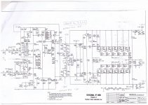
Q38 and Q50 actually control the output bias like in an Allison buffer. Q39 and Q51 appear to be a form of sequential startup circuit? They short the VAS output until the power rails are up, after which D26 and D3 are reverse biased.
Thanks, now that I look at it again, your explanation is good, wonder how that would simulate. I have seen the bias spreader get shorted out by a relay at start up, but that arrangement looks interesting.
Q39-Q51 and the additional diode-resistor network is responsible for soft clipping.Q38 and Q50 actually control the output bias like in an Allison buffer. Q39 and Q51 appear to be a form of sequential startup circuit? They short the VAS output until the power rails are up, after which D26 and D3 are reverse biased.
thank you very much for this information - I ask this question because a friend of me is owner of a damaged device with shorted output power transistors of this model from Mark Levinson.
Before ordering new devices I want to put this power amp into operation without the power output stage (i. e. only the front-end with Vbe multiplier drives the speakers - naturally in this kind I have a current control output with some mW power output).
This is the main step in my own troubleshooting procedure wich provide me a good protect to get additional shorted output transistors.
According the circuit description in post #57 follow prepare is necessary for getting this mode after removing the output (triplet follower) buffer:
1) node from R122/R121 together with speaker output terminals are to connect with C, Q25 resp. C, Q38
2) de-solder R49 and R24
If now DC conditions and idle currents in all stages from the front-end conclusive resp. according the showed values in schematic I will check the voltage range (bias) for the idle current in the output stage between C, Q25 and C, Q26 (must be between 3x0V45 and max 3x 0V75 for each half - i. e. between 1V35 and 2V25).
If this values are long time stable I connect speakers for sound check (extremely low level).
Let's see if I can do this and find the reason for the shorted power BjT's in the output buffer stage.
- Home
- Amplifiers
- Solid State
- Optimizing the VBE Multiplier