whatever you want to know...
I fiddled around with that chip 30years ago, also for a headphone amp, but I tossed it and got much better results with high current opamps.
Actually have been designing ultrasonic amps for Krautkraemer Huerth (USD10)
I fiddled around with that chip 30years ago, also for a headphone amp, but I tossed it and got much better results with high current opamps.
Actually have been designing ultrasonic amps for Krautkraemer Huerth (USD10)
Yes. And in my Modulus series I apply error correction to it using an LME49720. That's how I get the stellar performance.does this tomchr really uses 3886 in his design???
On some designs, yes.Also the plane is cut in smaller areas
That's flat out false. The current density will be the greatest in the direct path between source and load. It'll decay significantly once you move away from the direct path. By careful component placement, you can set up the layout to allow for a quiet section in the ground plane. Alternatively, you can slot or moat the plane.You just shouldn't use a grnd-plane on the combination power and pre.
The output currents then run all over the plane
You will get the best performance with a properly designed ground plane. But if you just draw a rectangle and hope for the best, you're not likely to get the best performance.
Tom
Last edited:
The LM3886 would not be my first choice for a headphone amp or an ultrasonic amp either. But neither of those appear to be OP's goal, so I'm not sure why they're relevant here.I fiddled around with that chip 30years ago, also for a headphone amp, but I tossed it and got much better results with high current opamps.
Actually have been designing ultrasonic amps for Krautkraemer Huerth (USD10)
Tom
Wow that is a nice design!
I wonder if it is possible to throw in another LM3886 in parallel to get more power out of this setup. Similar to official datasheet here - https://www.ti.com/lit/an/snaa021b/snaa021b.pdf
PCB has bunch of SMD elements - is it hard to solder those in? I am pretty new to diy audio and never worked with smd elements before.
Have anyone had experience with speaker protection boards using Omron relay? I wonder if it is actually worth it to include speaker protection circuit?
Thank you!
I suppose it could be done. You'd probably want to increase the value of R10-13, otherwise the load on U1a would be pretty low impedance (<500 ohms).I wonder if it is possible to throw in another LM3886 in parallel to get more power out of this setup.
I don't think it's difficult, but others disagree. You need a good pair of tweezers and some fine solder wire.PCB has bunch of SMD elements - is it hard to solder those in?
Mechanical relays aren't the best choice for speaker protection, as far as I know (assuming that's what you mean). MOSFET-based solid state relays are a better option.Have anyone had experience with speaker protection boards using Omron relay?
I don't use any protection circuit with my amp and it hasn't blown anything up (yet) 🙂

In the diy-hifi-forum is a thread with a pretty similar approach. https://www.diy-hifi-forum.eu/forum/showthread.php?10114-Balanced-Endstufen-mit-Chipamp
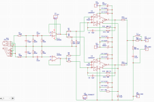
Here is the first revision of the concept that I was thinking would be a cool development on the schematics in the first post. The idea was to be able to power the amp using +/-35V. To do so, according to Tom from Neurochrome, we need to use two LM3886 chips so that they can share the load current.
Input buffers are just voltage followers - I am assuming they should not leak any DC to the inputs of the LM3886. I have DC blocking input capacitors before voltage followers for that purpose.
I wonder if it is possible to utilize servos in such configuration to reduce DC offset at the LM3886 outputs? Should it be hooked up to inverted, or non-inverted inputs of the LM3886?
Any thoughts or comments are welcomen 🙂
Attachments
Hello all,
I've published the design files for my balanced-input chip amp under an open license (CC BY-SA 4.0). The KiCad project files and Gerbers can be found in this GitHub repository. I've also included schematics in PDF (to make them viewable without installing KiCad). Documentation is, unfortunately, non-existent at the moment. I plan to add some documentation as well as BOMs in the future. Any comments/criticisms welcome.
You can see my build using these boards here.
I am little confused as to how you connected the input J1? If I were to assume that it is XLR balanced connection, then pin 1 is ground, pin 2 is positive, and pin 3 is inverted. According to the schematics, you feed pin 2 into the inverting input of the LM3886. So signals are flipped! Is that correct? Thanks
Yeah, I realized that soon after I sent the gerber files for fabrication... No big deal; the input terminals are labeled on the PCB. You can see that the wires are connected correctly in the linked photo of my build.
Regarding your schematic (I forgot to comment before):
I think you'll probably have a DC offset problem as shown. In my design, there are coupling caps between the input buffers and difference stage, which means that the effective DC gain of the LM3886 is unity. Ci in the datasheet application circuit does the same thing. In your design, the DC gain is 21. The typical and limit input offset voltages are 1mV and 10mV for the LM3886, so in your circuit the DC offset at the output could be as high as 210mV (not counting any DC from the input buffers).
You have R13 and R15 marked as 0.1% tolerance, but R7 through R12 should also be 0.1%.
The common mode input impedance is a bit low at 68.75kΩ.
As I understand, the schematics was inspired by the article "The G word" by Putzeys, Bruno. I just discovered it for myself a few weeks ago. It is pretty involved read, and I'm still trying to understand some parts of it. In particular, "The Diff Amp" under "Acting locally" section.
Also, I noticed that schematics by Bruno has pin 2 of XLR wired to the inverting pin of summing amp. My assumption is that it is on purpose and that I'm missing something here...
Also, I noticed that schematics by Bruno has pin 2 of XLR wired to the inverting pin of summing amp. My assumption is that it is on purpose and that I'm missing something here...
Assuming this is instrumentation amp configuration, the gain of the first stage at buffers is g = 1 + 2*1k / 2k = 2; the gain of difference amp LM3886 g = 10k/1k = 10. Total gain is equal 2*10 = 20. Is that correct?
I'm still trying to wrap my head around differential signaling. I'm confused if the gain needs to be multiplied by the factor of 2 since there are two signals that are being fed into LM3886? So the total gain is 40?
Don't you worry, this got me confused till some time not so far in the past. In fact if talking about 1V RMS differential usually there's "0.5V" RMS on the positive side (i.e. pin 2 of an XLR) and "-0.5V" RMS inverted on the negative side (pin 3 of an XLR) which will have a difference of 1V RMS exactly. It's all about differential - the difference between "0.5V" and "-0.5V" being exactly 1V.
Why I say usually? It might as well be "+1V" and "0V" on the two pins - or vice versa. It's still differential, just not balanced in that case.
Why I say usually? It might as well be "+1V" and "0V" on the two pins - or vice versa. It's still differential, just not balanced in that case.
It's still balanced and differential, but the signals are not symmetrical (see the "Take-home messages" box on page 3 of The G Word)It's still differential, just not balanced in that case.
No, it's still 20. If you have a 1V RMS symmetrical differential signal, you'll see 0.5V RMS on the + pin and 0.5V RMS (with reversed polarity) on the - pin. Why? Because a differential signal is the voltage difference between the two pins. 0.5V-(-0.5V)=1V.So the total gain is 40?
If you have a 1V RMS differential signal that is not symmetrical, the voltages will not be exactly opposite each other, but the difference between the two pins will still be the same. For example, you could have 1V RMS on the + pin and 0V on the - pin. The difference is still 1V-(-0V)=1V.
Correct me if I am wrong, here is the instrumentation amp formula:
Vout = (V1-V2) (1+2*R/Rgain) (Rf*Ri)
where V1 and V2 are diffential input voltage;
We can define the gain as A = (1+2*R/Rgain) (Rf*Ri)
Assuming differential signal of 1 Vrms per input:
On peak non-inverted V1 = 1Vrms
And inverted V2 = -1Vrms
Vout = (1-(-1)) * A = 2 Vpk * A
As a real life example, I have been reading review on Audio science review - Topping DX5 DAC
It shows balanced inputs at 4 Vrms per channel. So each balanced signal wire carries 4/2 = 2 Vrms?
RCA outputs are shown at 2 Vrms for each channel for that DAC.
Last edited:
Read my previous post again. I already answered your question.
A differential signal is never specified as "per input". The signal is the difference between two nodes. 1V RMS is 1V RMS. It doesn't matter if it's symmetrical or not.
A differential signal is never specified as "per input". The signal is the difference between two nodes. 1V RMS is 1V RMS. It doesn't matter if it's symmetrical or not.
Parts are in, so inspired by this thread I started my build 🙂 - not to clutter here is the link to the build with pictures - https://www.diyaudio.com/community/threads/balanced-input-lm3886-design-and-pcb-layout.386091/
- Home
- Amplifiers
- Chip Amps
- Open source balanced-input LM3886 design and PCB layout