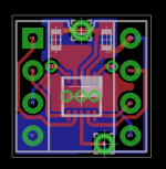
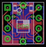
Revised my variant. Rotated the IC and switched the two op amps to allow for better routing. There seem to be two viable, geometric solutions (Olegs and mine). Changed the polygons for the thermal plane fill to be less "floody" around some corners.
- GND is connected to V- with a bridge between the left cap
- EN pin has a connector, and the trace can be cut to control it externally
- Big V- plane on bottom, small on top
- Board can be used "as-is" for DIP-8 replacement without sacrificing usability for prototyping
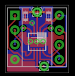
- GND is connected to V- with a bridge between the left cap
- EN pin has a connector, and the trace can be cut to control it externally
- Big V- plane on bottom, small on top
- Board can be used "as-is" for DIP-8 replacement without sacrificing usability for prototyping
Attachments
My experience with paste + stencil + hotplate soldering the OPA1622, was that I needed a couple of PCB revisions to optimize the polygons on the soldermask layer. %coverage and copper surround distance were fairly significant contributors to "%yield", where
%Yield = 100.0 * (# good boards) / (total # boards soldered)
So, I gently suggest building a low volume prototype run first, just to verify that you get high yield when soldering (a) on a hotplate; (b) with a hot air tool; (c) in a legitimate reflow oven. Then when you know all is well, launch the high volume PCB run.
Typical failure mechanism in my first revisions was pin-to-pin shorts.
Last edited:
Hi Mark, what you say is very true for commercial production runs.
But I'll only be doing a hobby/amateur PCB batch. Since I don't have access to a reflow oven anymore, I'll be soldering the few I want for personal use by hand anyway (hot air; at best).
The board lends itself for a group buy: With the normal minimum order for most fabs (10 boards of size 10x10cm each for 25USD + 19USD express shipping), I would get the tiny amount of 360 to 490 adapters.
Take away a few for myself plus some spares, I could send out about 100 packs of 4 boards each.
Regarding the layout/your yield: Good point. I suppose bigger copper areas close to the pins on the top layer contribute to pin-to-pin shorts?
If so, this should be mitigated by the layout attached to this post...
Attachments
Gosh that image in #23 is small, can you zoom it up to 900 pixels by 900 pixels?
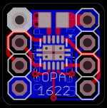
I got pin-to-pin shorts when hotplate soldering my OPA1622 boards, because there was too much solder paste on the heat spreader pad beneath the center of the package, and because the solder paste was too close to the edges of the PCB copper. Somehow it splashed or flowed or wicked over to other pads. Redesigning the soldermask layer (which my stencil vendor uses to create the stencil) improved this a lot.
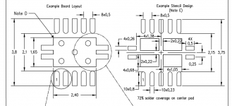
Attached is TI's example stencil layout. I found that 50% was better than 72% for highest soldering yield -- but I didn't run long term reliability experiments on finished adapter boards, making the OPA1622 pump out datasheet max current while operating at datasheet max Vcc and dataasheet max temperature.
I got pin-to-pin shorts when hotplate soldering my OPA1622 boards, because there was too much solder paste on the heat spreader pad beneath the center of the package, and because the solder paste was too close to the edges of the PCB copper. Somehow it splashed or flowed or wicked over to other pads. Redesigning the soldermask layer (which my stencil vendor uses to create the stencil) improved this a lot.
Attached is TI's example stencil layout. I found that 50% was better than 72% for highest soldering yield -- but I didn't run long term reliability experiments on finished adapter boards, making the OPA1622 pump out datasheet max current while operating at datasheet max Vcc and dataasheet max temperature.
Attachments
Hi Mark, exported at higher DPI.
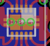
And nice insight! I think I could adapt the soldermask [tCream, gold] and solderstop [tStop, gray] layers to be a bit more narrow (assuming the fab can produce it). Attached is the original variant of the VSON10 pad from the eagle texas library.
Edit: Whoops, seems some things went wrong when I resized the board and moved it around. Updated the attached image to contain no obvious errors ;-)
Attachments
Last edited:
Attached are the finalized layouts of simplified and full featured adapter PCBs. Archives contain the gerber files.
Regards,
Oleg
Regards,
Oleg
Attachments
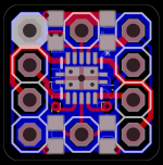
just a little observation on both ArchimedesMP and Oleg's designs.
pin 1 for the dip8 on Oleg's has a full silk screen over it and i dont think the fabricators will pass it. also you have radius corners, the fabricators will want to panellise the boards as they are so small.
the orientation indentation semi circle for the dip8 on ArchimedesMP board is the same as above as it runs over a pad (GND) as does the bottom line (V+).
I used such pin marking with silkscreen over the pad on my other designs produced by PCBWay. They never complained and PCBs were always fine. As for the panelization I would suggest not to use V-score since it is not precise and the groove can cut into the trace or pad. I would go with the CNC router cutting leaving small "bridges" between the boards instead. I think manufacturers can do such panelization on their own if you ask for it. In this case rounded edges are not a problem. Anyways, if someone decides to use the attached designs and needs them modified one way or the other just let me know.
It is always good to cross check, so thanks for looking at it.
In principle you expressed valid concerns🙂
In principle you expressed valid concerns🙂
Nice layouts guys!
Now if we can only find someone with the time, equipment and patience to assemble some of these.
I would certainly take a couple if the price isn't too high.
Otherwise, the '1622 won't be something I'll be trying.
Now if we can only find someone with the time, equipment and patience to assemble some of these.
I would certainly take a couple if the price isn't too high.
Otherwise, the '1622 won't be something I'll be trying.
Out of curiosity I checked how much it would cost to produce assembled OPA1622 adapter PCBs (simple version) using PCBWay assembly service. The prices are as follows:
100 boards: ~9.00 Euro/board
250 boards: ~7.00 Euro/board
Prices above include the adapter PCB itself, OPA1622 and one SMD ceramic capacitor per board (components supplied by the customer). No connectors included but these are cheap.
This means that if one would assume at least 20% faulty/lost on delivery units and add another couple of euros for paypal fees, diyaudio donation etc., then single board will cost no less than 13 Euro in quantity 100 and around 11 Euro in quantity 250. Add shipping and you have a full price.
That sounds quite reasonable to me considering the cost of the IC itself.
Will this replace a DIP-8 dual channel op-amp or is the pin configuration different?
Will this replace a DIP-8 dual channel op-amp or is the pin configuration different?
The simple adapter PCB is fully compatible with standard DIP8 dual channel op-amp pinout and needs no extra connections.
pcbway assembly...
Well I'll tell you what. 😀 If not possible to get a group buy together I would be willing to get 50 made at pcbway. The price per part would go up a bit with 50 instead of 100. But I would want to reserve the right to sell any extras out on eBay. 🙂
Some interesting (assembly) history: I used pcbway's assembly service last year to assemble some TPS3701 adapter boards, the ones I use in my Super CMOY projects. Came out great. I even had them use lead-free solder. I ordered 50. The TPS3701 wasn't available in china at the time (don't know if it is now), so I had Mouser do a Mouse Reel and shipped that to pcbway to use. They require 20 extra parts on the reel. Also found out that for boards that small pcbway can't machine-assemble they had to hand-assemble, but they came out looking great. I can't really tell the difference. I have the old email, but I think the minimum for machine assembly was 50mm x 50mm, plus a certain amount of extra around the edges.
All total I think it was around $120 for the chips from Mouser, $14 to ship them to china, $180 or so for the board fabrication and assembly which included pcbway supplying a small bypass cap on the board, Then the $21 DHL for the boards (and excess reel chips) back to the US.
I had extras listed out on eBay, can't remember if that is still up or not. 🙂
The cost for diyaudio'ers would be actual cost, plus actual shipping cost. Here in the US the shipping overseas is pricey. $13.50 is the cheapest from the US postal service, although I think Canada is a special case at $10. That is for the "first class parcel international" which is what they charge for anything that can't be run through a letter sorting machine.
One catch: like Mark says it would be best to hand-solder one to verify it works. I haven't got around to figuring out hot air soldering yet but I know someone who has (adydula) who I may be able to talk into soldering up a couple. 🙂 So what I would want to do is get some bare boards made first at pcbway, soldering them up, and test. For just small bare boards I may be able to get away with international letter rate at the post office by taping them to a piece of cardboard and saying I'm mailing a photo. 😀 I've had that work before. Letter rate is like $2 or so. Fabricating the bare test boards would be on me, I have some other stuff I need to send out to pcbway and I can combine shipping.
At any rate if any interest let me know. 🙂 A group buy would probably be the preferable way though if someone can put that together. I won't run group buys, I don't want to have other peoples money trapped for extended periods. 🙂
Also - regarding thickness - I did the first run of TPS3701 boards at 1.6 but that looked kind of chunky on such a small board. For the final run I went with 1.2mm. Still rigid but the proportions look a lot better.
Last edited:
If OlegSh is willing to do a group buy, or just send them out for fab/assembly himself, lets go that way! I would be in for several too. 🙂 I wouldn't be surprised if international shipping from most other countries beats the rates here. The USPS really needs a "small packet" international rate, something between $2 letter and $14 parcel.
Last edited:
The USPS really needs a "small packet" international rate, something between $2 letter and $14 parcel.
I agree. I've lost quite a few sales on my PCBs because of the $13.50 USPS international charge.
In most cases shipping is actually more than the price of the PCB.
- Status
- Not open for further replies.
- Home
- Amplifiers
- Headphone Systems
- OPA1622/VSON10 breakout board layout