I used TINA TI to simulate the OPA1622. Since the output trace of the OPA1622 on the PCB is relatively long, and there is an external protective relay connected to the 3.5mm headphone jack, plus the contact inductance of the relay, calculated as 1mm/1nh, this may cause 100nH As for the trace inductance, I connected a 100nH inductor in series to the output of the OPA1622, and then connected a 330pf capacitor to simulate the distributed capacitance of the headphone cable. I found that the gain margin was only 7.2 degrees. How can I increase the gain margin?
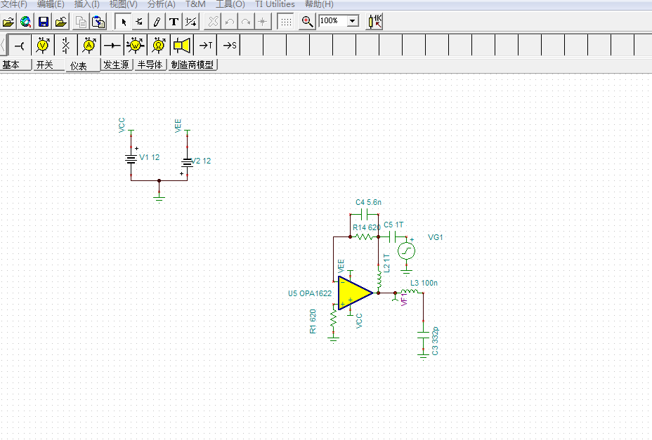
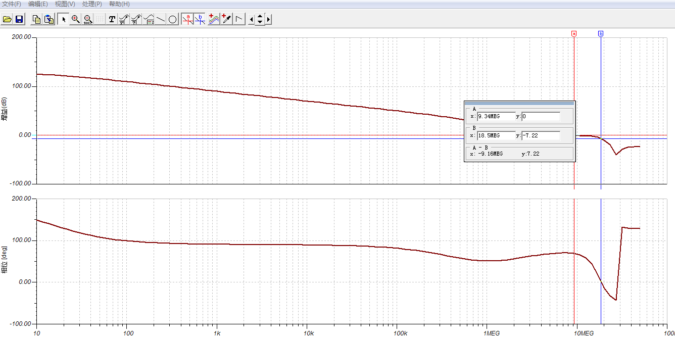
It is possible to obtain the open-loop gain of the op-amp (alone) from the closed-loop (actual) circuit, as Vout / (V+ - V-). Multiplying this value with the transfer of the feedback network would give the net loop gain of the circuit.
I don't know much of TINA, but I know that there's this post-processing function that may be used to write equations for displaying almost any (modelled) quantity.
I don't know much of TINA, but I know that there's this post-processing function that may be used to write equations for displaying almost any (modelled) quantity.
I checked some information and found that 7db is not enough. Since the opa1622 output pcb trace is relatively long and the contact length of the relay causes inductance, this may cause loop instability.
I also found a problem. Using TINA simulation, the phase margin of opa1622 under 1nf capacitive load does not seem to match the datasheet figure 24, which is about 20 degrees higher.
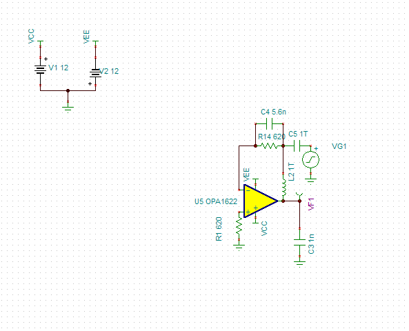
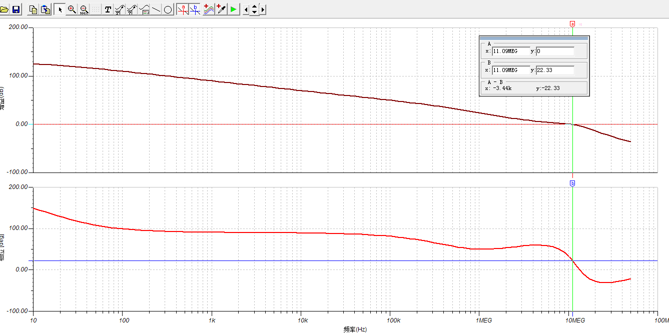
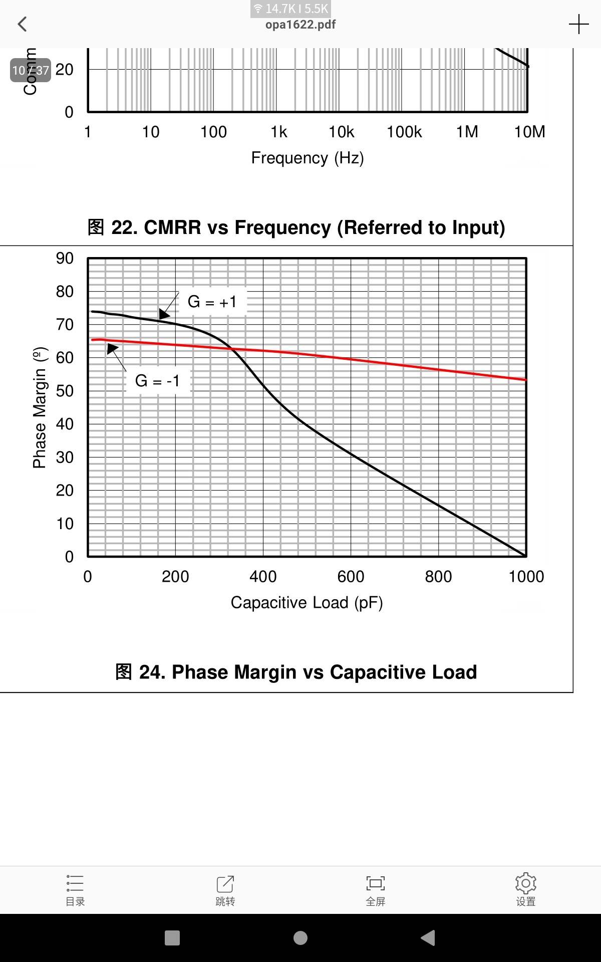
I also found a problem. Using TINA simulation, the phase margin of opa1622 under 1nf capacitive load does not seem to match the datasheet figure 24, which is about 20 degrees higher.
Tried adding 1k and 100 ohms in parallel and found that only less than 100 ohms would be stable.could also be the resonance of the output LC starting to show up or an effect of the purely reactive load. Try adding some resistive load.
Yep. TINA supports equations.I don't know much of TINA, but I know that there's this post-processing function that may be used to write equations for displaying almost any (modelled) quantity.
Figure 24 is with 2 kΩ load (says the text at the top of the page). I interpret that as 2 kΩ || Cload for Fig. 24. I'd also imagine that Rf = 0 Ω and Cf = none.Using TINA simulation, the phase margin of opa1622 under 1nf capacitive load does not seem to match the datasheet
Tom
2k ohm results are the same
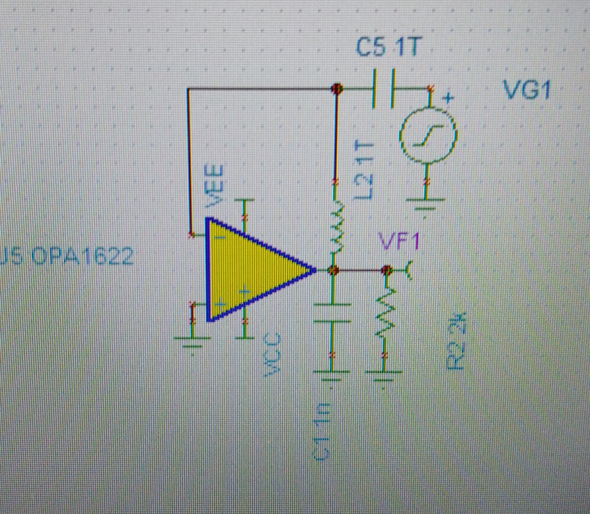
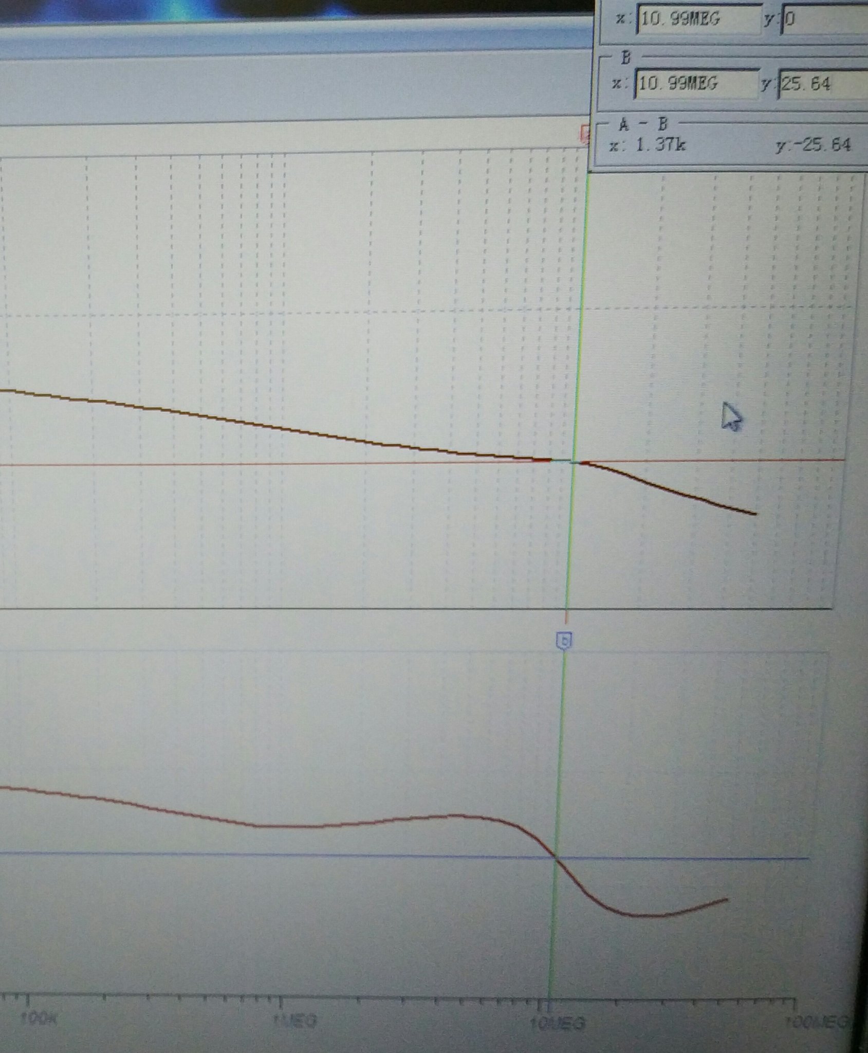
2k ohm results are the sameFigure 24 is with 2 kΩ load (says the text at the top of the page). I interpret that as 2 kΩ || Cload for Fig. 24. I'd also imagine that Rf = 0 Ω and Cf = none.
2k ohm parallel connection, cf=0, rf=0r, 1nf load, phase margin is not 0, does not comply with datasheet figure 24Figure 24 is with 2 kΩ load (says the text at the top of the page). I interpret that as 2 kΩ || Cload for Fig. 24. I'd also imagine that Rf = 0 Ω and Cf = none.
This sort of issue is usually tamed by adding a small value capacitor between output and inverting input close to the chip. Suggest modelling that and figuring out how many pF are likely to be needed.
Similar issues can happen with layout that has too much stray capacitance between output and non-inverting input - again adding capacitance between output and inverting input can fix this. There's a solid reason for the standard pinout for dual and quad opamps - the output is next to the inverting input, not to the non-inverting input.
Similar issues can happen with layout that has too much stray capacitance between output and non-inverting input - again adding capacitance between output and inverting input can fix this. There's a solid reason for the standard pinout for dual and quad opamps - the output is next to the inverting input, not to the non-inverting input.
Tried it but it didn't workThis sort of issue is usually tamed by adding a small value capacitor between output and inverting input close to the chip. Suggest modelling that and figuring out how many pF are likely to be needed.
Similar issues can happen with layout that has too much stray capacitance between output and non-inverting input - again adding capacitance between output and inverting input can fix this. There's a solid reason for the standard pinout for dual and quad opamps - the output is next to the inverting input, not to the non-inverting input.
According to TI, output series resistance makes distortion largerThere is no resistor in series with the opamp output. It is usual to put about 47 ohms right close to the output pin to ensure stability with reactive loads.
Having used this device extensively in a number of designs, and have read the datasheet from end to end I can find no mention of an increase in distortion (which is vanishingly small anyway for this device) as a result of a small value series resistor.
I would always add a series resistor to isolate an opamp from capacitive loads. 47 ohms is really a minimum when the load environment is unknown or high. Usually in an audio application - like a preamp - 100 ohms is more common, or even higher in series with the output.
Anyway you have an ideal capacitor and ideal inductor, with no losses. It is little wonder that the model borders on instability.
This article explains the effect of series resistance.Having used this device extensively in a number of designs, and have read the datasheet from end to end I can find no mention of an increase in distortion (which is vanishingly small anyway for this device) as a result of a small value series resistor.
I would always add a series resistor to isolate an opamp from capacitive loads. 47 ohms is really a minimum when the load environment is unknown or high. Usually in an audio application - like a preamp - 100 ohms is more common, or even higher in series with the output.
Anyway you have an ideal capacitor and ideal inductor, with no losses. It is little wonder that the model borders on instability.
https://www.ti.com/lit/pdf/slyt630
I measured the headphone cable to be 1.5Ohm and the total capacitance of the PCB trace to be 360~375pf. When I input these parameters into TINA TI, the stability margin is still not enough.
OK - what the article makes clear is that the impedance curve of the headphones acts with a series resistor to give a modified frequency response, which is absolutely true.
But his distortion mechanism has at its root his statement "...the current drawn by headphone drivers is not perfectly linear..." "...thus distorting the current drawn by the driver." So his calculated distortion curves with a series resistor is a result of that mechanism.
His mechanism of using an input snubber is essentially introducing a noise gain at higher frequencies, which (a) reduces the hf bandwidth (not a bad thing) and (b) improves stability margin. There is a similar technique of using an output snubber, perhaps in combination with an input snubber.
Note that his article relates to a differential input from a DAC, and yours is single ended - although an input snubber would work there too. Have you tried that?
Last edited:
It has nothing to do with the DAC as this is the loop of the OPA1622 itself. I have actually built it, using a 4-layer PCB, using 0.8mm traces for the output, with a length of 45mm. Including the relay, the total length is almost 60mm, and the trace distance is 0.2mm from the second layer of ground. It sounds like there is no problem, but the simulation results of TINA TI worry meOK - what the article makes clear is that the impedance curve of the headphones acts with a series resistor to give a modified frequency response, which is absolutely true.
But his distortion mechanism has at its root his statement "...the current drawn by headphone drivers is not perfectly linear..." "...thus distorting the current drawn by the driver." So his calculated distortion curves with a series resistor is a result of that mechanism.
His mechanism of using an input snubber is essentially introducing a noise gain at higher frequencies, which (a) reduces the hf bandwidth (not a bad thing) and (b) improves stability margin. There is a similar technique of using an output snubber, perhaps in combination with an input snubber.
Note that his article relates to a differential input from a DAC, and yours is single ended - although an input snubber would work there too. Have you tried that?
- Home
- Amplifiers
- Chip Amps
- OPA1622 PCB trace inductance causes gain margin issues