Hello all.
This Onkyo M-5030 amplifier has almost fully separated channels (only speaker protection circutry is connecting them) and has a history of burning down one channel...
I worked on it first in 2020 when it had burnt the channel output transistors the second time in a short period (according to the owner).
The previous technician had replaced the output transistors with ones salvaged from another amplifier and also some of the ceramic capacitors.
But both output transistors in one leg of the channel shorted again.
OK, I replaced the whole set with "pulled originals" from eBay, checked other components and the amplifier started up again.
It worked (not in frequent use) ok for ca two years but about half a year ago it was "dead" again - power transitors again.
Some resistors had visual signs of overheating.
I also unsoldered and measured all surrounding components and more than one resistor open.
Long story short - I started to power the amplifier up carefully proceeding step by step.
The VAS stage on regulated power (with output transistors unpowered) acted OK - no oscillation, no excess currents.
Time to connect the power transistors - I placed 100R 10W resitors in B+ an B- rails (to the power stage) and everything was OK.
Why not use a variac or DBT?
The VAS stage gets itself powered via regulatros which do not work with lower mains voltage (Onkyo dropped that complexity in later models and did not use it earlier if my memory serves me correct):

So far so good.
But when I replaced the rail resistors with 10R ones then "magic smoke" was let out.
To my surprise the output transistors measure (in disconnected from board state) ok with a DMM (in diode mode) but at least one 0,33R ceramic resistor in their collector lines is cracked.
Now the next step is to check all components again but after that all advice is welcome how to proceed with poering the amplifier without burning it again.
So guys, walk with me ...
This Onkyo M-5030 amplifier has almost fully separated channels (only speaker protection circutry is connecting them) and has a history of burning down one channel...
I worked on it first in 2020 when it had burnt the channel output transistors the second time in a short period (according to the owner).
The previous technician had replaced the output transistors with ones salvaged from another amplifier and also some of the ceramic capacitors.
But both output transistors in one leg of the channel shorted again.
OK, I replaced the whole set with "pulled originals" from eBay, checked other components and the amplifier started up again.
It worked (not in frequent use) ok for ca two years but about half a year ago it was "dead" again - power transitors again.
Some resistors had visual signs of overheating.
I also unsoldered and measured all surrounding components and more than one resistor open.
Long story short - I started to power the amplifier up carefully proceeding step by step.
The VAS stage on regulated power (with output transistors unpowered) acted OK - no oscillation, no excess currents.
Time to connect the power transistors - I placed 100R 10W resitors in B+ an B- rails (to the power stage) and everything was OK.
Why not use a variac or DBT?
The VAS stage gets itself powered via regulatros which do not work with lower mains voltage (Onkyo dropped that complexity in later models and did not use it earlier if my memory serves me correct):
So far so good.
But when I replaced the rail resistors with 10R ones then "magic smoke" was let out.
To my surprise the output transistors measure (in disconnected from board state) ok with a DMM (in diode mode) but at least one 0,33R ceramic resistor in their collector lines is cracked.
Now the next step is to check all components again but after that all advice is welcome how to proceed with poering the amplifier without burning it again.
So guys, walk with me ...
Yes, there was nothing alarming. Also the transistors did not heat up abnormally - I monitored them with an infrared thermometer (and also with a finger tip).Did you measure the rails with the 100R resistors in place?
You need output transistors not from ebay!
Use equivalent modern transistors from Mouser or digikey,replace the drivers too.
A common fault reason is the Q404=VD1212 in the bias circuit.This is here for temperature compensation but if this fail, (resistor jump) bias is full and outputs burned.
Use equivalent modern transistors from Mouser or digikey,replace the drivers too.
A common fault reason is the Q404=VD1212 in the bias circuit.This is here for temperature compensation but if this fail, (resistor jump) bias is full and outputs burned.
Attachments
The current set is modern, also the drivers if I remember correctly.Use equivalent modern transistors from Mouser or digikey,replace the drivers too.
I will unsolder them all and check.
Please read D404 not Q404.You need output transistors not from ebay!
Use equivalent modern transistors from Mouser or digikey,replace the drivers too.
A common fault reason is the Q404=VD1212 in the bias circuit.This is here for temperature compensation but if this fail, (resistor jump) bias is full and outputs burned.
Sorry.
No problem, I will just start checking the components, it will take some time. All resistors in the output stage need to be checked too - last time I found a couple of defective ones which had no visual indication of being damaged.Please read D404
I believe this is an Onkyo specialty.last time I found a couple of defective ones which had no visual indication of being damaged.
I have often had this happen and at Luxman too.
While checking components a question:
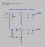
should I replace the zener and fet (from regulator transistor collector side to base)

with a resistor like in A-8250:

so that I could use variac and DBT while testing?
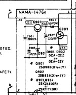
Onkyo seems to have solved this circuit in very many ways in its different models - with a resistor, with a fet, with a zener, with zener and fet (amples are in the attached images)...
should I replace the zener and fet (from regulator transistor collector side to base)
with a resistor like in A-8250:
so that I could use variac and DBT while testing?
Onkyo seems to have solved this circuit in very many ways in its different models - with a resistor, with a fet, with a zener, with zener and fet (amples are in the attached images)...
Attachments
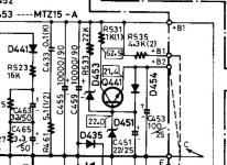
OK, finished component check in the outpt stage.
As suspected by thimios, D404 is open.
Other transistors and resistors (except a cracked ceramic 0,33R resistor on one output transistor collector) are fine.
Question: what should I use for replacement or could these diodes just be eliminated?

As suspected by thimios, D404 is open.
Other transistors and resistors (except a cracked ceramic 0,33R resistor on one output transistor collector) are fine.
Question: what should I use for replacement or could these diodes just be eliminated?
Another question:
Where should such diodes (or transistors) be actually placed?
The original placement of D404 seems to have been on the collector lead from the output transistor.
It would be easier to attach it on the plastic body of the transistor.
But some amplifier models have used transistors in such a regulation function which is pressed/bolted on the heatsink some centimeters away from the output transistors.
So how fast reacting these diodes should actually be?
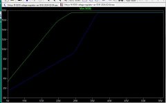
OK, did a simulation in LTspice - seems that I need ca 40V as B+/- in order to have proper regulated voltage for VAS.
Question is - is 40V (on rails) a safe starting point (when using a variac)?
Question is - is 40V (on rails) a safe starting point (when using a variac)?
Attachments
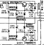
OK, time to start planning powering it up - D404 showed intermittent results when diode-chacking plus it also showed ca 30pF capacitance.
I replaced it with two 1N4148 diodes as recommended in more than one thread in internet.
So how should I power it up - via variac and through DBT?
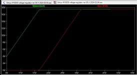
Or perhaps use variac for powering regulated voltage rails with regulators bridged with 4k7 resistors - then it is possible to get nominal voltage when feeding the amp with less than 50% of the mains voltage (green line is 1 k resistor, blue is 4,7 k resistor, red is "no resistor").:

- and powering the output stage from a regulated external (adjustable) power supply?
Or am I overcomplicating things and should proceed with the known 100R in power rails route?
I replaced it with two 1N4148 diodes as recommended in more than one thread in internet.
So how should I power it up - via variac and through DBT?
Or perhaps use variac for powering regulated voltage rails with regulators bridged with 4k7 resistors - then it is possible to get nominal voltage when feeding the amp with less than 50% of the mains voltage (green line is 1 k resistor, blue is 4,7 k resistor, red is "no resistor").:
- and powering the output stage from a regulated external (adjustable) power supply?
Or am I overcomplicating things and should proceed with the known 100R in power rails route?
Time to warm up the iron again...
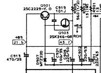
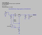
About thermocoupling D404 to the output transistors:
M-5060 is a predecessor of M-5030 (as far as I could learn from the net) and similar diode D4009 in Vbe multilpier:

is located on the board (Q4013 is mounted on heatsink):

In m-5030 Q413

is mounted on heatsink (i.e. thermally copled to the outputs) while also D404 has originally been glued to the collector ping of an output transistor.
After replacement of the outputs in one channel I glued (with thermo-glue) these diodes to the plastic body of the output transistor:

So with replaced diodes it would look like this:

Is such an arrangement really necessary or is it over-engineering from that time?
I do not remember many amplifiers (not that I have seen too many but still) with such diodes been placed/mounted on the heatsinks...
Edit:
Found a nice video on Youtube explaining visually how Vbe works:
About thermocoupling D404 to the output transistors:
M-5060 is a predecessor of M-5030 (as far as I could learn from the net) and similar diode D4009 in Vbe multilpier:
is located on the board (Q4013 is mounted on heatsink):
In m-5030 Q413
is mounted on heatsink (i.e. thermally copled to the outputs) while also D404 has originally been glued to the collector ping of an output transistor.
After replacement of the outputs in one channel I glued (with thermo-glue) these diodes to the plastic body of the output transistor:
So with replaced diodes it would look like this:
Is such an arrangement really necessary or is it over-engineering from that time?
I do not remember many amplifiers (not that I have seen too many but still) with such diodes been placed/mounted on the heatsinks...
Edit:
Found a nice video on Youtube explaining visually how Vbe works:
Last edited:
Proceeding in small steps and moderate tempos.
Should I test the output transistors under power (to measure their possible leakages etc) would it be best to short the driver transistors' bases or short them while connecting to ground?
Idea is to have the VAS stage unpowered.
Schematics is at post #11.
Should I test the output transistors under power (to measure their possible leakages etc) would it be best to short the driver transistors' bases or short them while connecting to ground?
Idea is to have the VAS stage unpowered.
Schematics is at post #11.
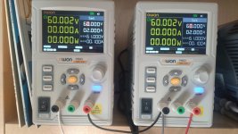
Powering up - step 1:
B+ and B- to output transostors, driver transistor Q414/415 bases shorted and overcurrent sensing tranistor feed resistors R464(465 lifted - 0 mA current @60V , at least it is not smoking or burning...

B+ and B- to output transostors, driver transistor Q414/415 bases shorted and overcurrent sensing tranistor feed resistors R464(465 lifted - 0 mA current @60V , at least it is not smoking or burning...
Attachments
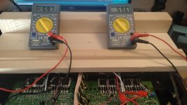
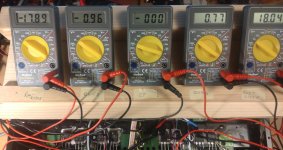
Powering up - step 2:
B+ and B- to VAS and Vbe stage (these have separate wiring from main capcitors than output transistors and their drivers).

Regulated voltages reach nominal values at 40 V, current draw is stable around 50 mA @60V:

So far, so good.
B+ and B- to VAS and Vbe stage (these have separate wiring from main capcitors than output transistors and their drivers).
Regulated voltages reach nominal values at 40 V, current draw is stable around 50 mA @60V:
So far, so good.
Attachments
- Home
- Amplifiers
- Solid State
- Onkyo M-5030 burnt channel rebuild