As the film title says, “Never say never”.
So perhaps I should not have used the word last attempt.
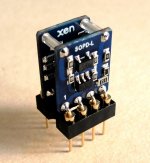
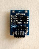
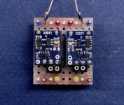
Anyhow, a DC-stable discrete opamp in a DIP-8 Footprint has remained unfinished business for me, despite a few attempts over the years.
The previous failures were largely due to DC offsets and unity-gain stability.
In the last 18 months, after much contemplation, a renewed effort was made to take on this challenge one last time.
This time with much better success, apparently.
Nothing really ground breaking. But that is also not where the difficulty lies.
Patrick
.
So perhaps I should not have used the word last attempt.
Anyhow, a DC-stable discrete opamp in a DIP-8 Footprint has remained unfinished business for me, despite a few attempts over the years.
The previous failures were largely due to DC offsets and unity-gain stability.
In the last 18 months, after much contemplation, a renewed effort was made to take on this challenge one last time.
This time with much better success, apparently.
Nothing really ground breaking. But that is also not where the difficulty lies.
Patrick
.
Attachments

Time to move to pre-biased transistor arrays in SOT1216 package perhaps? 🙂
https://assets.nexperia.com/documents/data-sheet/PQMD10.pdf
https://assets.nexperia.com/documents/data-sheet/PQMD10.pdf
Precisely what I do not want to do.
1) cross-over distortion, as in any commercial IC opamps
2) extra components required for biasing
3) thermal tracking difficulties of NPN to PNP
The only advantage is more driving capabilities.
For typical line level applications with 10k load, 8mA NJFET Source Follower is more than enough.
But it is only my personal design choice.
Others might have other choices.
Patrick
the dominant pole in these circuits are the BJT PNP stages. Ft/beta.
ever considered a high Ft pnp pair like the HFA3135 .these need cascoding for voltage compliance. also good to reduce for early voltage distorsion.
ever considered a high Ft pnp pair like the HFA3135 .these need cascoding for voltage compliance. also good to reduce for early voltage distorsion.
A few issues here :
1) Not easily available. No stock at Digikey & Mouser.
2) Hfe 5x lower than the ones used.
3) NF 3~4dB higher
And do you have a spice model for those ?
Patrick
1) Not easily available. No stock at Digikey & Mouser.
2) Hfe 5x lower than the ones used.
3) NF 3~4dB higher
And do you have a spice model for those ?
Patrick
I find it so interesting to read your design decisions as to what would work better and why. Often the 'why' doesn't get explained which makes it so much harder to learn.
Good luck with it and please keep feeding us lurkers 😉
Good luck with it and please keep feeding us lurkers 😉
you could start simming with a BFT92, just to see if you can move GBW up, to improve slew with less capacitance.
Not exactly what you wanted, but RF PNP users cannot be choosers today.
*-----------------------------------------------------------------------------
* Siliconics / Renesas HFA3046/3096/3127/3128 Transistor Array SPICE Models
* SOI process Rev. 1.0 February 1994 Appnote MM3046.pdf 9 & 5.5 GHz ft
* ghf: in the next line they wrote PUHF also... must have been misprint
.model NUHFARRY NPN
+ (IS = 1.840E-16 XTI = 3.000E+00 EG = 1.110E+00 VAF = 7.200E+01
+ VAR = 4.500E+00 BF = 1.036E+02 ISE = 1.686E-19 NE = 1.400E+00
+ IKF = 5.400E-02 XTB = 0.000E+00 BR = 1.000E+01 ISC = 1.605E-14
+ NC = 1.800E+00 IKR = 5.400E-02 RC = 1.140E+01 CJC = 3.980E-13
+ MJC = 2.400E-01 VJC = 9.700E-01 FC = 5.000E-01 CJE = 2.400E-13
+ MJE = 5.100E-01 VJE = 8.690E-01 TR = 4.000E-09 TF = 10.51E-12
+ ITF = 3.500E-02 XTF = 2.300E+00 VTF = 3.500E+00 PTF = 0.000E+00
+ XCJC = 9.000E-01 CJS = 1.150E-13 VJS = 7.500E-01 MJS = 0.000E+00
+ RE = 1.848E+00 RB = 5.007E+01 RBM = 1.974E+00 KF = 0.000E+00
+ AF = 1.000E+00 )
*
.model PUHFARRY PNP
+ ( IS= 1.027E-16 XTI= 3.000E+00 EG= 1.110E+00 VAF= 3.000E+01
+ VAR= 4.500E+00 BF= 5.228E+01 ISE= 9.398E-20 NE= 1.400E+00
+ IKF= 5.412E-02 XTB= 0.000E+00 BR= 7.000E+00 ISC= 1.027E-14
+ NC= 1.800E+00 IKR= 5.412E-02 RC= 3.420E+01 CJC= 4.951E-13
+ MJC= 3.000E-01 VJC= 1.230E+00 FC= 5.000E-01 CJE= 2.927E-13
+ MJE= 5.700E-01 VJE= 8.800E-01 TR= 4.000E-09 TF= 20.05E-12
+ ITF= 2.001E-02 XTF= 1.534E+00 VTF= 1.800E+00 PTF= 0.000E+00
+ XCJC= 9.000E-01 CJS= 1.150E-13 VJS= 7.500E-01 MJS= 0.000E+00
+ RE= 1.848E+00 RB= 3.271E+01 RBM= 9.902E-01 KF= 0.000E+00
+ AF= 1.000E+00 )
*
At this moment, I am quite happy with the design as they are.
And I have bad experiences with HF devices.
I am not in a spec race, which I shall not win anyway.
So if anything, only the 4V/µs slew rate (required for unity gain stability) is a touch low.
But that still gives me almost 1MHz at 1Vrms out at G=1.
At G=10, bandwidth is no longer slew rate limited.
It is still a healthy 300kHz.
I guess quite sufficient for most applications.
I could also reduce the amount of compensation, if I do not need to have unity gain stability.
But that would be customising.
All devices, especially the dual ones, are active parts and readily available.
And all are very low noise.
Patrick
> Often the 'why' doesn't get explained which makes it so much harder to learn.
These are results of 18 months' work and many iterations.
So there is no straight forward explanation for everything.
Sometimes it is just a random choice by gut feeling.
Sometimes trial and error.
Of course you can always ask.
I'll see if I can give a rational answer.
And thanks for the interest,
Patrick
There's no such thing for at least 30 years in audio op-amps on a chip.Precisely what I do not want to do.
1) cross-over distortion, as in any commercial IC opamps
Patrick
It's only the chip technology that allows the class b output stages to have no crossover distortion and finally beat the class a in discrete technology on this aspect.If you're going to measure anything, i bet that you're going to do it with the aid of an ic with zero crossover distortion. Again, there's no benefit in having smd components on a pcb of a chip size...New smd chips have thermal pads that allow considerable heat dissipation .
- Home
- Source & Line
- Analog Line Level
- One Last Attempt at Discrete Opamp in DIP8 Footprint