good morning I apologize if I insert myself brutally... The simulations did not show these distortions...
I would like to know what difference you found between measured THD and THD from LTSpice
If it were a high value this would seem worrying to me.
If there is low correlation even for such a basic circuit i wonder what could happen with more complex ones
Did you use a model provided by a manufacturer and buy the specific component?
Could there be problems with the model?
I built this up in sim early in the thread but it didn't fit the criteria and then discussion shifted to the 317 circuit, and I never posted it. Using Barry Blesser's "Super Transistor" (h/t Scott Wurcer) and @MarcelvdG's idea of CRDs, I tried to stay within the bounds of the original criteria as much as possible. I think this would require one trace cut in the original circuit, at the original base. The top side (schematic-wise) of the cut would connect to the collector-base junction, the bottom side to the input emitter. I never saw details on the source and load impedances. I used 9.56k from original schematic as load R, and tested with 50, 1k, and 10k source impedances. I did not breadboard as I have no CRDs.
I used the Central Semi CRDs because their Spice models were easy to access. The CCL0130 models give 90uA rather than the expected 130uA. After checking the datasheet, 90uA looks about right for 27C, with 130uA at a higher temp (high, positive tempco--may require a different R5 value, a parallel resistor, or be unusable in real world application). Qspice sim attached, models embedded. For other programs, Central Semi CRD model file attached (CCL.txt), and BJTs are the Cordell models.
Sim results (when three values given, read as RS=50/1k/10k):
-Input impedance (ohms): 116K with variance <1k across frequency.
-Gain(dB) @ 1k: -0.005/-0.08/-.72
-Frequency Response: <-.04dB at 20hz
-Input referred noise @ 1kHz (nV/rtHz): 2.8/6.3/34.8
-Input referred noise @ 20Hz (nV/rtHz): 8.1/9.9/35.6
-SNR ref 1Vrms (dB): 128/122/108
-THD1k 1Vrms (dB): -119/-111/-96
-THD1k 5Vrms (dB): -78/-68/-52
-THD20k 1Vrms (dB): -102/-92/-76
-THD20k 5Vrms (dB): -78/-67/-51
FR can be flattened by increasing output C. LF Noise rise can be reduced by increasing input C. 47u for both caps gets rid of both issues.
THD is primarily 2H. Lowest load resistance that does not clip with 7.071Vpk input is 1.5k.
Input impedance is parallel of R5 and the super-transistor's "base" at emitter Q1. At LF, the impedance looking into Q1 emitter is approximately Beta(Q2)*RL, but at megaohms like you get with 10k load, it's less (presumably early effect and output impedance of current source).
Attachments

I can't find many of the Central Semi CRDs for sale either (well I havent emailed the sales team at central semi, their website shows in stock). Here are E-101 and E-103, equivalent to the CCL0130 and CCLH100 respectively.
https://www.mouser.com/ProductDetail/Semitec/E-101?qs=wgO0AD0o1vvz3gt6ABxxUg==
https://www.mouser.com/ProductDetail/Semitec/E-103?qs=wgO0AD0o1vvf%2BAlP9/JcaQ==
https://www.mouser.com/ProductDetail/Semitec/E-101?qs=wgO0AD0o1vvz3gt6ABxxUg==
https://www.mouser.com/ProductDetail/Semitec/E-103?qs=wgO0AD0o1vvf%2BAlP9/JcaQ==
Last edited by a moderator:
thanks again ! found !
https://www.mouser.it/ProductDetail/Semitec/E-101?qs=wgO0AD0o1vvz3gt6ABxxUg==
i dont understand how they work to be honest Do they act limiting or setting the current flowing through them ?
from what you write they change properties with T ? can be replaced by resistors ?
anytime i see something zen i am confused and excited at the same time
Sorry for the broken links above. The current regulating diodes act as two terminal current sources, so they send a (relatively) fixed current. Internally, they are self-biased JFETs. See attached app note for info on this technique.
Attachments
Last edited:
Sorry to go off topic This is a 2 bjts circuit Very classic but it seems that almost nobody consider it Why ?
https://www.electronics-notes.com/images/transistor-two-device-amplifier-circuit-01.svg
when optimized it should have low THD and low Zout I do not about its PSRR
i wonder if it could be done with same 2 npn
https://www.electronics-notes.com/images/transistor-two-device-amplifier-circuit-01.svg
when optimized it should have low THD and low Zout I do not about its PSRR
i wonder if it could be done with same 2 npn
That's a CFP with gain, tends to underperform quite a bit compared to CFP follower, as the feedback is too heavily loaded - you either have poor THD or R4/R5 have to dissipate a lot more power than you would like to linearize the feedback path (i.e. swamp the non-linear current demand of TR1). If you make R4 << R5 you have only a small bit of gain, but this can be handy for getting the most out of the supply rails, and its more linear as its almost a follower.Sorry to go off topic This is a 2 bjts circuit Very classic but it seems that almost nobody consider it Why ?
https://www.electronics-notes.com/images/transistor-two-device-amplifier-circuit-01.svg
when optimized it should have low THD and low Zout I do not about its PSRR
i wonder if it could be done with same 2 npn
Hi thank you very much indeed for your kind and valuable advice
With the precious help of Mr Mooly i am trying to simulate it with LtSpice (at present i am still learning about settings and other things)
As soon as i will be able to use the SW correctly i will change values as you suggest for sure
Thank you very much again
With the precious help of Mr Mooly i am trying to simulate it with LtSpice (at present i am still learning about settings and other things)
As soon as i will be able to use the SW correctly i will change values as you suggest for sure
Thank you very much again
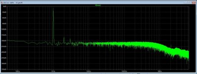
Hi i have tried the schematic but using resistors and the THD spectrum at 1kHz at least looks quite nice (i wonder about its limits)View attachment 1307161
I built this up in sim early in the thread but it didn't fit the criteria and then discussion shifted to the 317 circuit, and I never posted it. Using Barry Blesser's "Super Transistor" (h/t Scott Wurcer) and @MarcelvdG's idea of CRDs, I tried to stay within the bounds of the original criteria as much as possible. I think this would require one trace cut in the original circuit, at the original base. The top side (schematic-wise) of the cut would connect to the collector-base junction, the bottom side to the input emitter. I never saw details on the source and load impedances. I used 9.56k from original schematic as load R, and tested with 50, 1k, and 10k source impedances. I did not breadboard as I have no CRDs.
I used the Central Semi CRDs because their Spice models were easy to access. The CCL0130 models give 90uA rather than the expected 130uA. After checking the datasheet, 90uA looks about right for 27C, with 130uA at a higher temp (high, positive tempco--may require a different R5 value, a parallel resistor, or be unusable in real world application). Qspice sim attached, models embedded. For other programs, Central Semi CRD model file attached (CCL.txt), and BJTs are the Cordell models.
Sim results (when three values given, read as RS=50/1k/10k):
-Input impedance (ohms): 116K with variance <1k across frequency.
-Gain(dB) @ 1k: -0.005/-0.08/-.72
-Frequency Response: <-.04dB at 20hz
-Input referred noise @ 1kHz (nV/rtHz): 2.8/6.3/34.8
-Input referred noise @ 20Hz (nV/rtHz): 8.1/9.9/35.6
-SNR ref 1Vrms (dB): 128/122/108
-THD1k 1Vrms (dB): -119/-111/-96
-THD1k 5Vrms (dB): -78/-68/-52
-THD20k 1Vrms (dB): -102/-92/-76
-THD20k 5Vrms (dB): -78/-67/-51
FR can be flattened by increasing output C. LF Noise rise can be reduced by increasing input C. 47u for both caps gets rid of both issues.
THD is primarily 2H. Lowest load resistance that does not clip with 7.071Vpk input is 1.5k.
Input impedance is parallel of R5 and the super-transistor's "base" at emitter Q1. At LF, the impedance looking into Q1 emitter is approximately Beta(Q2)*RL, but at megaohms like you get with 10k load, it's less (presumably early effect and output impedance of current source).
Low 2nd and lower 3rd
Thanks a lot for the recommendation
Attachments
Hi it's me again I did as you recommended i.e. using the cfp as a buffer and ended with a very clean 1kHz THD spectrumThat's a CFP with gain, tends to underperform quite a bit compared to CFP follower, as the feedback is too heavily loaded - you either have poor THD or R4/R5 have to dissipate a lot more power than you would like to linearize the feedback path (i.e. swamp the non-linear current demand of TR1). If you make R4 << R5 you have only a small bit of gain, but this can be handy for getting the most out of the supply rails, and its more linear as its almost a follower.
I tried as a preamp as well but could not reach below - 100dB
However i have decided to switch to opamps after all advices got in this sense and also because i have seen a very high end manufacturer passing from full discrete designs to opamps in their very latest and best line preamp
Off topic ... i have seen measurements on a very high end preamp of the past and was amazed by the high level of THD Maybe there were some parts out of specs i dont know It can be come out from factory with those figures
Attachments
Hi please excuse me if i disturb you But i have open the Cordell models list and found very interesting models that i would like to add to the default library of LTSpiceView attachment 1307161
I built this up in sim early in the thread but it didn't fit the criteria and then discussion shifted to the 317 circuit, and I never posted it. Using Barry Blesser's "Super Transistor" (h/t Scott Wurcer) and @MarcelvdG's idea of CRDs, I tried to stay within the bounds of the original criteria as much as possible. I think this would require one trace cut in the original circuit, at the original base. The top side (schematic-wise) of the cut would connect to the collector-base junction, the bottom side to the input emitter. I never saw details on the source and load impedances. I used 9.56k from original schematic as load R, and tested with 50, 1k, and 10k source impedances. I did not breadboard as I have no CRDs.
I used the Central Semi CRDs because their Spice models were easy to access. The CCL0130 models give 90uA rather than the expected 130uA. After checking the datasheet, 90uA looks about right for 27C, with 130uA at a higher temp (high, positive tempco--may require a different R5 value, a parallel resistor, or be unusable in real world application). Qspice sim attached, models embedded. For other programs, Central Semi CRD model file attached (CCL.txt), and BJTs are the Cordell models.
Sim results (when three values given, read as RS=50/1k/10k):
-Input impedance (ohms): 116K with variance <1k across frequency.
-Gain(dB) @ 1k: -0.005/-0.08/-.72
-Frequency Response: <-.04dB at 20hz
-Input referred noise @ 1kHz (nV/rtHz): 2.8/6.3/34.8
-Input referred noise @ 20Hz (nV/rtHz): 8.1/9.9/35.6
-SNR ref 1Vrms (dB): 128/122/108
-THD1k 1Vrms (dB): -119/-111/-96
-THD1k 5Vrms (dB): -78/-68/-52
-THD20k 1Vrms (dB): -102/-92/-76
-THD20k 5Vrms (dB): -78/-67/-51
FR can be flattened by increasing output C. LF Noise rise can be reduced by increasing input C. 47u for both caps gets rid of both issues.
THD is primarily 2H. Lowest load resistance that does not clip with 7.071Vpk input is 1.5k.
Input impedance is parallel of R5 and the super-transistor's "base" at emitter Q1. At LF, the impedance looking into Q1 emitter is approximately Beta(Q2)*RL, but at megaohms like you get with 10k load, it's less (presumably early effect and output impedance of current source).
In the default library there are many smd bjts that i will never use I am quite lost about adding the models I have looked at some tutorials but they are more and more confused Again the models by Mr Cordell are very good parts
If you aware of any clear tutorial i would be very grateful
Thanks a lot again and kind regards
gino
another low THD buffer option taken from the vintage Kenwood 700C preamp output buffer (with the original dual supply replaced by a single lower V supply. I was curious to see because i read great things about this very old preamp that was Kenwood's totl preamp in 1975)
i know ... with opamps is easier
The problem is that many bjts present in the stock library are smd ... i have no clue about how to add the more popular bjts that can be found everywhere like BD139 all the Toshibas ... MJE182 ... ecc.
i know ... with opamps is easier
The problem is that many bjts present in the stock library are smd ... i have no clue about how to add the more popular bjts that can be found everywhere like BD139 all the Toshibas ... MJE182 ... ecc.
Attachments
You can find models here for example:
https://ltwiki.org/index.php?title=Standard.bjt
You can copy one model from the list, and paste it directly on the schematic, like this:
If you need many of the models from the list, you can copy and paste it into the lib file named standard.bjt in the CMP folder.
They will make them automatically available for any simulation.
The Kenwood circuit is yet again a CFP
Attachments
Note that the "best" bias point for a passive pull up/down amplifier is 33% not 50%, because the if the load and pull-up/down are the same then the passive current peak is half the active current peak.
I simulated over a dozen buffer circuits, including an op-amp, and the best result was a complimentary P-P EF buffer.
I simulated over a dozen buffer circuits, including an op-amp, and the best result was a complimentary P-P EF buffer.
- Home
- Source & Line
- Analog Line Level
- One BJT line amp/buffer