Values I proposed previously are with headphones output in mind. Downside is increased dissipation and large components (Q1 and R4). For less demanding load (worse performance with headphones) you can use BC547 and R4=3k3 1/4W. In that case, replacing R4 with e.g. 2SK246 (any similar jfet with Idss 4-8mA) with source and gate shorted could improve THD an order of magnitude.
LM317 is a good idea to.
LM317 is a good idea to.
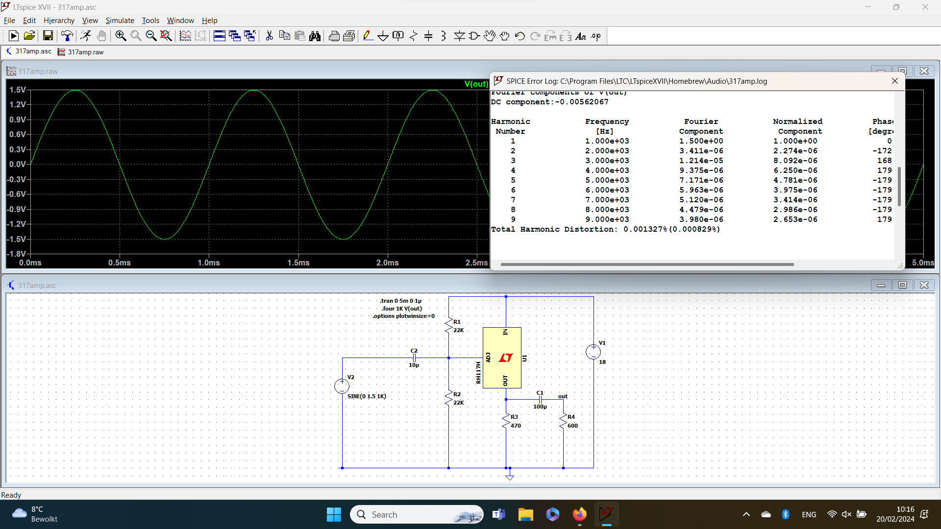
This is the 317 version:

It fits the bill and has vanishingly low THD. In reality, some small capacitors or RC networks might be required for stability
It fits the bill and has vanishingly low THD. In reality, some small capacitors or RC networks might be required for stability
GOOD news
I stopped somehow the presumable oscillations (100pF in B-C) and distortions were mended.
Now, at 1V input I have H2 at -60dB and H3 at -80dB and SNR>110dB.
For curiosity, later I disconnected the capacitor but the harmonics (oscillations) did not reappear. Strange. Maybe there was a rest of solder somewhere and now it fell off.
I will also try the JFET current source in place of R4. Should I also change BC550 to BC549 (sizeable bigger)?
Will also try the LM317: LV, what type should them better be? Standard TO-220 or LVHP (metal can TO-39)?
If you can find a -L version (TO92) or -M version (TO39 or TO202), they should be OK for light loads.Will also try the LM317: LV, what type should them better be? Standard TO-220 or LVHP (metal can TO-39)?
The regular TO220 type is OK too, even for lower power, if you can accommodate the larger case
Just a question, maybe very silly:This is the 317 version:
- here too one can split the R3 in two (R3' and R3") and replace the lower side (R3") with a constant current source (JFET GS shorted). Then take FB from middle node and run it from there via R1 (hence lower pin not on GND)?
- The output is also from middle node, via a large decoupling C. Load to ground!
Would this CCS-style inspired topology work? Any advantage in terms of noise or something? (Maybe it needs an OpAmp follower in the FB).
I cannot simulate or draw, as LM317 model not here and my time is very short until weekend.
The CCS could have a R14K short to ground, just in case the load is disconnected.
The R3' should be correctly scaled, in the low range(?).
I don't see clearly what you want to achieve with FB or splitting. Remember, this is a non-inverting unity gain buffer.
Replacing R3 with a CCS is possible, and might bring a tiny improvement in performance, but it is really not worth the trouble: the output impedance of the 317 is less than 0.1 ohm
Replacing R3 with a CCS is possible, and might bring a tiny improvement in performance, but it is really not worth the trouble: the output impedance of the 317 is less than 0.1 ohm
not sure myself either. Maybe to make a NFB (via an inverting follower in FB) and so to mind oscillations...?Remember, this is a non-inverting unity gain buffer.
Or maybe better THDs and noise?
Will it be self-DCbiasing?
I must not talk or write until I get myself the LM317 model and time to play. Will plan this for weekend.
Thanks for input!
...And dissipation. With R4 = 470R, dissipation on the active element is over 200mW which might be demanding for L version (TO92 pack). TO220 is OK.Mind the minimum load current.
I must say that I want to retreat from this topic for a while, although the subject itself remains probably interesting for others.
How easy is to make this one-BJT have a NF of 10dB, when in DS it tells 1.2dB? Or, how easy for BJT amateurs like me to not understand things properly? Reverse, how hard is to understand things right in the BJT world?
This is what I measured today: a decrease in SNR of 10dB, Output vs Input. The schematic and values were those which I posted at the beginning. I wanted to document the situation as reference before applying your ideas and see changes.
I will continue to experiment your ideas. Thanks! Maybe I will improve with time at my end.
How did you arrive at/compute that noise figure?
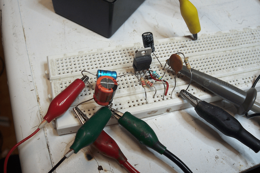
In the meantime, I have tested the 317 version in real life:

As was more or less expected, I had to add a stabilization network across the 470ohm output sink: 10ohm + 10nF.
I didn't try to optimize anything, as it worked immediately.
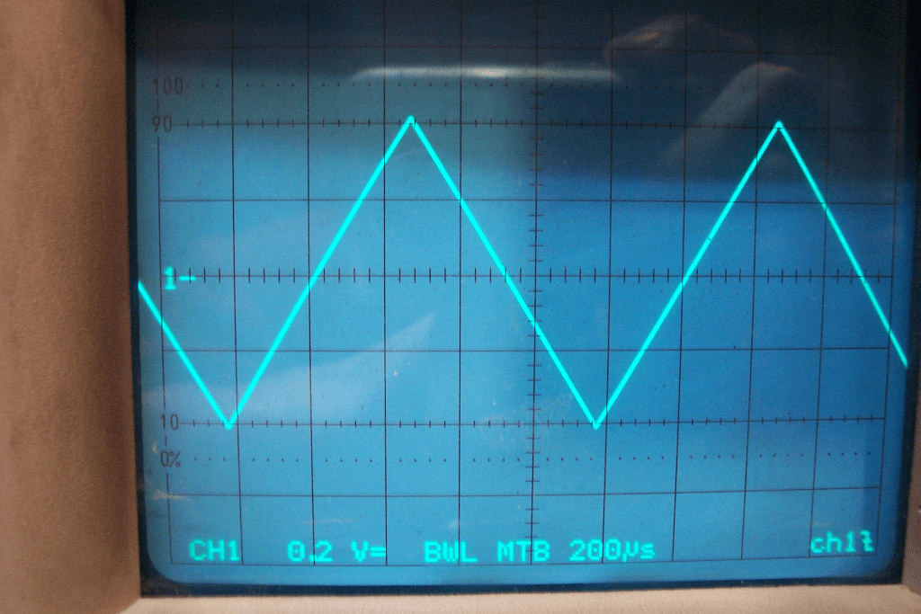
This is the result, with a 1kHz triangle signal:

Pretty neat. I may measure the THD later
In the meantime, I have tested the 317 version in real life:
As was more or less expected, I had to add a stabilization network across the 470ohm output sink: 10ohm + 10nF.
I didn't try to optimize anything, as it worked immediately.
This is the result, with a 1kHz triangle signal:
Pretty neat. I may measure the THD later
The LM317 circuit works well.
I got THD 0.00007% in a simulation of 1 Vp into 600 Ohm.
But check the frequency ressponse,
I got THD 0.00007% in a simulation of 1 Vp into 600 Ohm.
But check the frequency ressponse,
The simulated THD is certainly overoptimistic; even the 0.0013% predicted by LTspice probably (slightly) is.
From my previous Vreg amplifiers experience, I can infer that the full power bandwidth will reach 20 to 40kHz; not exceedingly ample, but perfectly sufficient for the reproduction of audio programs having undergone transmission, encoding, decoding, pre+deemphasis, etc.
From my previous Vreg amplifiers experience, I can infer that the full power bandwidth will reach 20 to 40kHz; not exceedingly ample, but perfectly sufficient for the reproduction of audio programs having undergone transmission, encoding, decoding, pre+deemphasis, etc.
I must say that I want to retreat from this topic for a while, although the subject itself remains probably interesting for others.
How easy is to make this one-BJT have a NF of 10dB, when in DS it tells 1.2dB? Or, how easy for BJT amateurs like me to not understand things properly? Reverse, how hard is to understand things right in the BJT world?
This is what I measured today: a decrease in SNR of 10dB, Output vs Input. The schematic and values were those which I posted at the beginning. I wanted to document the situation as reference before applying your ideas and see changes.
I will continue to experiment your ideas. Thanks! Maybe I will improve with time at my end.
By definition, the noise figure is only equal to the loss of signal-to-noise ratio when the source has a defined impedance and a noise corresponding to the thermal noise of the real part of that impedance at a temperature of 290 kelvin (16.85 degrees Celsius).
If your signal source fits that description, could you specify the source impedance, measurement band and weightings (if any), so we can interpret the noise figure properly?
If not, could you explain how you measured that 10 dB SNR loss?
For the circuit of post #1, the thermal noise of R1 and the shot noise of the base current of Q1 are likely to be the dominant noise sources, if the supply is perfectly clean. Both should be negligible for a line level amplifier, though, when the source impedance is reasonably low.
Indeed, a very beautiful triangle 🙂 I will try it myself.
How I came to the SNR (from memory):
If Impedance is constant, then the NF definition still applies, if my understanding is right? This is what I tried to do.
Instrumentation: PicoScope 4262 (up to 5MHz, 16-24 bit) as Oscilloscope, SA and Source.
How I came to the SNR (from memory):
- set SA: BW 20KHz, filter LP 200KHz.
- set the SA in the lowest sensitivity for 16bit (10mV).
- preset the Source level: amplitude 7,75mV (-40dB) @1000Hz. Check that signal is not over driving the SA input.
- ProbeA (x1) alone: Noise floor at ca. -138dBu (probably ca 4000 points)
- ProbeA on Amp In: Amp On / Source Off : -117dBu. This is noise floor of measurement (Amp Power supply On, etc)
- ProbeA on Amp In: Amp On / Source On : -113dBu. This is the Amp IN with noise from Source (pretty good in specs, according to DS). Signal -40dBu.
- ProbeB on Amp Out (RCA-to-Coax 50 Ohm adapter): Amp On / Source On: -103dBu. This is the Amp OUT. Signal still -40dBu (as expected).
If Impedance is constant, then the NF definition still applies, if my understanding is right? This is what I tried to do.
Instrumentation: PicoScope 4262 (up to 5MHz, 16-24 bit) as Oscilloscope, SA and Source.
if the Signal Source is clean or if the power supply is clean?For the circuit of post #1, the thermal noise of R1 and the shot noise of the base current of Q1 are likely to be the dominant noise sources, if the supply is perfectly clean. Both should be negligible for a line level amplifier, though, when the source impedance is reasonably low.
I am not sure if the source impedance is 0.1Ohm or 50Ohm (at audio frequencies).
Port A and B are identical, BNC format.
- Home
- Source & Line
- Analog Line Level
- One BJT line amp/buffer