chas
How did you get in this "fxo = 9kHz therefore (630 /9E3) X 48 = mod gain = 3.4 or 1.5 db" 3.4 to 1.5dB
How did you get in this "fxo = 9kHz therefore (630 /9E3) X 48 = mod gain = 3.4 or 1.5 db" 3.4 to 1.5dB
Luka
Luka
The f(xo) = crossover frequency choosen by designer.
The Flc = 630 Hz which is 1 / 6.28 * SQR of L * C using 32uH for
inductor and 2000 uF for capacitor.
To calculate the gain is Vin = bulk supply (max) in EU = about 380VDC
Vs = ramp voltage of SG3525 about 2.5 VDC from datasheet
Ns = number of secondary turns of transformer
Np = number of primary turns of transformer
I choose a transformer with Ns = 7T and Np = 22 turns therefore
the calucation for Flc = 629.4 Hz or 630Hz
the DC gain = Vin /Vs * Ns/Np = numeric 48 or 34 db (20 log * 48)
the gain at flc is 630HZ / 9kHZ * 48(numeric value of DC gain) = 3.36 or 10.5 db ( my error sorry)
The DC gain is 48 or 34 db
The gain at Flc is 10.5 db
This is covered in Marty Brown's "Power Supply Cookbook" pg#202 thru 219
chas1
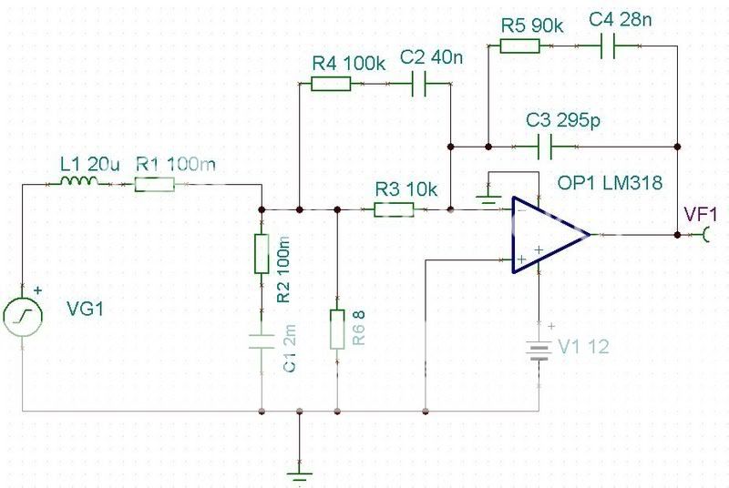
this is what I have now
L=20uH
C=2000uF
Fxo=6kHz
Fep1=2.5kHz
Fep2=25kHz
Fez1,2=398Hz
Flc=796Hz
Npri=24
Nsec=7
Vin=330v, not max value
Vs=2.5v
DC gain=38.5 numeric
Gain at Fcl =5.1 numeric
So I get
A1=9
A2=0.9
R1=10k (my choise)
R2=90k
R3=100k
C1=295p
C2=28n
C3=40n
Am I even close here on this values?
L=20uH
C=2000uF
Fxo=6kHz
Fep1=2.5kHz
Fep2=25kHz
Fez1,2=398Hz
Flc=796Hz
Npri=24
Nsec=7
Vin=330v, not max value
Vs=2.5v
DC gain=38.5 numeric
Gain at Fcl =5.1 numeric
So I get
A1=9
A2=0.9
R1=10k (my choise)
R2=90k
R3=100k
C1=295p
C2=28n
C3=40n
Am I even close here on this values?
FLC
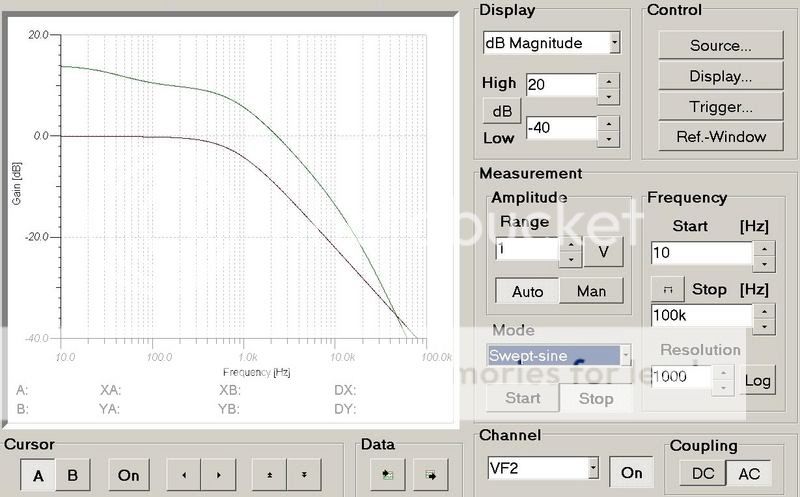
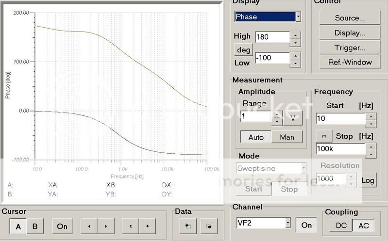
Luka the plots look ok, but you need to calcuate your flc, I think you have your two zero's below the corner frequency. How did you get a value 398Hz. The formula is 1 / 6.28 * SQRT L* C from your values of 20uH for inductor and 1000 each for caps I get a flc of 796Hz and I think you might want to place the two zero's here. Another Item is to plot the output filter without the series resistor's for these are not real values ; while the inductor does have a dc resistance and as well the capacitor does have a ESR these value's must be measured to include them in the schematic unless your intent is to place physical resistor's in the circuit. I have heard of people who do this but I don't think it's necessary in MHOP.
chas1
Well for Fez1,2= Fcl/2 or as in book Ffp, I think... You have that on pg#217 in eq B.34, and I do too get for Fcl=796Hz
I have no way of measuring any resistance that small, so I will remove resistors from the plot graf.
It look's good... I thought I was way off 😀
So what now? Should I build this one, how do I connect it to SG?
Now I like this: When output voltage is right opto puts Vref to one of the inputs of op in SG, other one is Vref/2 all the time.

slow response
Luka
I am sorry for the slow response, but need time to draw schematic and explain. Will finish later today.
chas1
Luka
I am sorry for the slow response, but need time to draw schematic and explain. Will finish later today.
chas1
Chas
Would it be possible to do feedback with TL431 like you did for fullbridge?
And if yes is it as good as with OP amp?
Would it be possible to do feedback with TL431 like you did for fullbridge?
And if yes is it as good as with OP amp?
feedback loop
Luka
I would like to go over your schematic and comment on some items:
1. R5C4 is the first zero FZ1 and the results of the calculation equals 63Hz.
2. R3C2 is the second zero FZ1 and the results of the calculation equals 398Hz.
3. R4C2 is the first pole FP1 and the results of the calculation equal 39Hz.
4. R5C3 is the second pole FP2 and the results of the calculation equal 5396Hz.
You will not be able to assign a value to R3 as it is the upper resistor in the voltage divider that provides the feedback from Vout. (Example Vout is 35 volts and you use a reference of 5 volts then R3 becomes 30K and the lower leg will be 5K if you allow 1ma of current thru the divider.
The low frequency gain (DC) is determined by R5/R3 and this must raise the gain of the fxo to 0 db.
Your FLC is 798Hz, then a pole at 2.5 kHz and the last pole above 1/2 fs.
You should place the two zeros at the FLC so the fx0 will be on a slope of 20db.
I am enclosing a schematic from Brown’s book that uses the opto and the tl431.
To test this circuit you breadboard it and use a bench supply and vary the voltage +/- 2 volts around 35 volts and measure pin 11 or 14 of the SG3525 as you go above 35 volts the pulse should narrow and as you go below 35 volts it should widen and at 35 volts the duty cycle should be about 50%. You only need low voltage for this test (12 volts to supply Sg3525 and use the 5 volts from pin 16 for the collector voltage of transistor.
chas1
Attachments
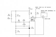
I have some difficulty reading shematic, there are different elements marked the same R3,R5,C2,...
But I think I can read through,R3 and R3 in series... are there to set output voltage, right?
But I think I can read through,R3 and R3 in series... are there to set output voltage, right?
error on schematic
Luka
The schematic has error's but the two R3 are the voltage divider and the R3 to ground is the lower resistor ; the other is from your schematic. Note this circuit is set up for a 2.5 volt reference.
chas1
Luka
The schematic has error's but the two R3 are the voltage divider and the R3 to ground is the lower resistor ; the other is from your schematic. Note this circuit is set up for a 2.5 volt reference.
chas1
I gues this is it. Just what I need to bring the beast to its full potencial... 🙂
I do have 2.5 volt reference.
At this point I start to ask myself what else can go wrong? Is there anything?
I do have 2.5 volt reference.
At this point I start to ask myself what else can go wrong? Is there anything?
connection
Luka
take a look at the datasheet, you can't disable the error amp so to get around then connect the output (pin9) to the inv input(pin1).
chas1
Luka
take a look at the datasheet, you can't disable the error amp so to get around then connect the output (pin9) to the inv input(pin1).
chas1
One more question. Do I connect it over +/- voltage,as we did the simulation this way, or not?
And for caps I did buy 270p for 295p, 33n for 28n and 33 for 40n.Now do I have to re-cal the values of resistors?
And for caps I did buy 270p for 295p, 33n for 28n and 33 for 40n.Now do I have to re-cal the values of resistors?
Connection
Luka
I only connect the feedback to the postive output . The negative output should follow the postive output since they are Symmetrical.
The values of the resistor's might need to be changed , this depends on the response of your feedback loop. before you connect it to your supply check it with a 500mv pulse input and look at the output should show no evidence of distortion or ringing.
chas1
OOps I forgot to rewire the secondary side of optocoupler. That is whay I get narrow pulses when output voltage is low 😀
Have to correct this
Have to correct this
- Home
- Amplifiers
- Power Supplies
- Offline full-bridge SMPS… need help