Hi Ashok,
Thanks for the enquiry,
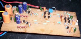
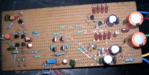
The Design is Fully ready to serve the Diyers, I have built & tested it.... 🙂
Further refinements are possible if there is a keen interest in this Design shown by you guys...its upto you friends....
K a n w a r
Thanks for the enquiry,
The Design is Fully ready to serve the Diyers, I have built & tested it.... 🙂
Further refinements are possible if there is a keen interest in this Design shown by you guys...its upto you friends....
K a n w a r
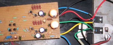
How about some oscilloscope captures of square wave behaviour, high frequency clipping behaviour, etc... and some pictures of the prototype?
Dear Kanwar, now i am travelling, when return , i will construct your amplifier......
And will be happy to listen to it.
Congratulations, very nice design.
regards,
Carlos
And will be happy to listen to it.
Congratulations, very nice design.
regards,
Carlos
Alleluia, all have sung? I do not wish to offend.!Workhorse said:Hi Folks,
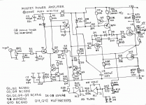
Here's the final design Simply enjoy!
K a n w a r
what for? The second äèôêàñêàä, the **** LAST YEAR'S.
if, on N-channel, IMHO, the best variant.
p,s. Translation, I am sorry.!
Attachments
Hi VAD,
Your circuit is using P-Channel as driver and will definately exhibit cross-conduction when loaded with paralleled large number of mosfets at the output and also if subjected to no-load condition also.....that is an open circuit operation....
Secondly, its neither has rail to rail output thus efficiency is some what lower....
Whereas in my circuit, all bipolar transistors are small signal ones, low cost...solution
Rail to rail output for increased efficiency..thats what mosfets are choosen for.....
Push pull drivers for Zero cross-Conduction even at no load or with parallel bank of output mosfets up to 10Pairs....
K a n w a r
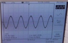
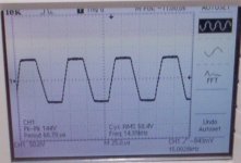
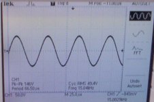
Isn't such a thick trace a sign of rampant and copious oscillation? Note that you are watching at 50V/div so the trace has something like 5V p-p of noise!!
Your oscilloscope features 40Mhz or better bandwidth, 1Gs/s sampling and 8 bit resolution in a 240 pixel height display, so it should show a crisp clear waveform at 15Khz (if the original waveform wasn't really noisy, of course...)
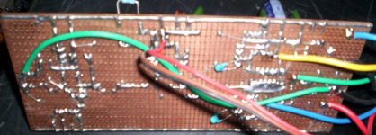
Anyway, with such long and spaced leads connecting the PCB to the output devices and such a wide spread layout, oscillation is very likely to happen. Note that even with the very tight layout that I employed in my N-channel prototype (all the output stage and supply decoupling concentrated in a 4cm by 4cm rectangle), I had to solve some oscillation issues.
Also, you don't have to get a camera and take photos of the actual display in order to publish your waveforms. It should be possible to connect your oscilloscope to a computer through a simple RS-232 wire and use the software package from the manufacturer to get high quality digital images of your measurements. I find that system very useful for storing and comparing results, documenting projects, showing circuit performance to other people, etc...
That's exactly what I do with my oscilloscope (Hameg HM-407), this thread shows some captures: http://www.diyaudio.com/forums/showthread.php?postid=848584#post848584
Your oscilloscope features 40Mhz or better bandwidth, 1Gs/s sampling and 8 bit resolution in a 240 pixel height display, so it should show a crisp clear waveform at 15Khz (if the original waveform wasn't really noisy, of course...)
Anyway, with such long and spaced leads connecting the PCB to the output devices and such a wide spread layout, oscillation is very likely to happen. Note that even with the very tight layout that I employed in my N-channel prototype (all the output stage and supply decoupling concentrated in a 4cm by 4cm rectangle), I had to solve some oscillation issues.
Also, you don't have to get a camera and take photos of the actual display in order to publish your waveforms. It should be possible to connect your oscilloscope to a computer through a simple RS-232 wire and use the software package from the manufacturer to get high quality digital images of your measurements. I find that system very useful for storing and comparing results, documenting projects, showing circuit performance to other people, etc...
That's exactly what I do with my oscilloscope (Hameg HM-407), this thread shows some captures: http://www.diyaudio.com/forums/showthread.php?postid=848584#post848584
Hi Eva,
The Thick trace is not oscillation but a "Waveform Display feature in scope" just to increase the width for displaying the waveform more easy for the camera to capture....
No-Oscillations at all.....😉 but noise was there ofcourse...which too gets widening with width incrementing....
The noise coupling was actually from the source of Waveform generator and its not from the amp output.....itself...
Yes the leads are long but donot put the amp into oscillations....
Yes the TEK Scope offers a Centronics port for connecting to PC for much illustration of waveforms, but i havent configured it yet ....
K a n w a r🙂
Workhorse said:Hi VAD,
Your circuit is
Just for the record - it is not his circuit but mine 🙂 . More precise it is a version of my circuit I've used for Creek Audio 4330 amplifier in 1997.
using P-Channel as driver and will definately exhibit cross-conduction when loaded with paralleled large number of mosfets at the output and also if subjected to no-load condition also.....that is an open circuit operation....
Secondly, its neither has rail to rail output thus efficiency is some what lower....
Whereas in my circuit, all bipolar transistors are small signal ones, low cost...solution
Rail to rail output for increased efficiency..thats what mosfets are choosen for.....
Push pull drivers for Zero cross-Conduction even at no load or with parallel bank of output mosfets up to 10Pairs....
K a n w a r
My circuit is desiged for 40 W per channel into 8 Ohm, about 70 W into 4 Ohm. It is simple and the power supply usage is fairly good - about the same as in your circuit with one pair of output devices. One important notice - in my circuit the open loop output impedance of the output stage is low (less than 0.2 Ohm) - this seriously helps the sound when the amp works on real-world speakers. Also I've found from my experience that both paralleled devices and source resistors are bad for the sound 🙂 .
So each design has it's own goals and strong points - yours too. That is why there are so many different circuits.
Cheers
x-pro
- Status
- Not open for further replies.
- Home
- Amplifiers
- Solid State
- NVMOS amplifier