Workhorse, here I am home again, I see the thread has been busy 😉
First of all, regarding changes of the bootstrap cap with a voltage source, I was just using that as an experiment. Besides, it would not change anything as far as driving goes as using a bootstrap cap is exactly for the reason that you are impersonating a voltage source with it. I am still not sure why you would lose headroom on the low end if it was one resistor, but the question is academic as the driver has other issues. Fortunately darkenfriz has provided a solution to it, and more:
With the original circuit:
1) potentially very serious, if the driver stage fails to provide the driving current for any reason, the outputs are fully biassed ON (= lots of smoke!).
2) driver LTP must be able to swing down very close to -V rail if you want to switch off the lower transistor, which requires a very low voltage reference for it's CCS. At 100 deg C for high threshold MOSFETs you are looking at close to 2V up from -V, this could have been a problem. The current mirror approach solves this.
Darkenfriz, I would say that the top MOSFET in the original schematic was also a current cource (disregarding the PSRR issue for now) as it's driving voltage was locked ONLY to the driver stage current and not to the output voltage, by virtue of the bootstrap cap. In other words, the output impedance of the top half is also very high. It is certainly true in you implementation with current mirrors.
I still have an issue with the bias generator. I think Darkenfriz is on the right path as the IRF610 will definitely do a good job of thermal tracking. However, the circuit has gain from Vgs of the thermal sensing MOSFET to the output MOSFETs Vgs, equal to Rgs _outputs / 2*Rgs_ccs. Thermal tracking depends on this 'gain' as the thermal gradient of Vgs threshold is also amplified. This is always the tricky bit with such topologies.
I once had such a problem and this is how I solved it:
1) You need the voltage on the CCS current sense resistor (the one across IRF610 G and S) to track equally with the bias Vgs of the output MOSFETs. In order to do so your MOSFETs need to have proportional Vgs threshold, or the tracking will be off. The simple solution is to aim for equal threshold, which means you need to chose the sensing MOSFET that is built on the same cell technology as the output MOSFETs. In this case, gain will be ~~1 and Rgs_ccs ~~ Rgs_output/2. In other words: carefully evaluate the MOSFETs to use and adjust the CCS 'gain', you cannot just use any resistance ratio.
2) Consider adjusting the idle current by adjusting the resistor* that feeds the junction of the base of the BJT and the drain of the IRF610 in the CCS. Increasing the current requires increase of the IRF610 Vgs, which provides the means of adjustment. At the same time, the current sensing resistor remains the same, and so does the Vgs 'gain' of the CCS with respect to the output MOSFETs.
*At first glance one would expect a constant current source to be a better choice in this place, but in fact a simple resistor has the ability to compensate changes of MOSFET Gm with Vds, which apply equally for the CCS MOSFET as for the output MOSFETs. In order to use this 'feature', MOSFETs built on the same cell technology have to again be chosen.
You also want to reduce idle current modulation by power supply droop. In order to do this, split the adjusting resistor into two and connect the midpoint to -V rail through a large cap (in other words, add PSRR to the CCS by bootstrapping it's reference)
One more thing, I was just looking at making the design two stage by using a full LTP for the second stage, and a PNP folded cascode to drive the outputs but the bias generator on that requires some inspired analysis...
ilimzn said:Darkenfriz, I would say that the top MOSFET in the original schematic was also a current cource (disregarding the PSRR issue for now) as it's driving voltage was locked ONLY to the driver stage current and not to the output voltage, by virtue of the bootstrap cap. In other words, the output impedance of the top half is also very high. It is certainly true in you implementation with current mirrors.
Yes, you're right.

Hi Kanwar
You sure you would not be partaking of some illicit herbs? This is worth doing, right? SIMPLE. I don't think so.
You sure you would not be partaking of some illicit herbs? This is worth doing, right? SIMPLE. I don't think so.
amplifierguru said:Hi Kanwar
You sure you would not be partaking of some illicit herbs? This is worth doing, right? SIMPLE. I don't think so.
here comes the Guru, welcome to this thread , kindly expand your views in non jargonmatic illustration.😉 😀 😀
Seriously Kanwar,
This folly of yours is starting to look like 'one with the lot' - great for marketing I'm sure. Let's see, it's got N CHANNEL, it's got FOLDED CASCODE, it's got RAIL to RAIL ( does it still have that?), it's got SIMPLICITY ( no it lost that way back), it's got OPTOCOUPLED bias (coming),....
It's also got complex thermals, electro's in the signal path, and DC offset? It's got THD? It's got slewing? It's got COMPLEXITY.
It's DIY scary is what it is. GLADIATOR indeed.
amplifierguru said:Seriously Kanwar,
This folly of yours is starting to look like 'one with the lot' - great for marketing I'm sure. Let's see, it's got N CHANNEL, it's got FOLDED CASCODE, it's got RAIL to RAIL ( does it still have that?), it's got SIMPLICITY ( no it lost that way back), it's got OPTOCOUPLED bias (coming),....
It's also got complex thermals, electro's in the signal path, and DC offset? It's got THD? It's got slewing? It's got COMPLEXITY.
It's DIY scary is what it is. GLADIATOR indeed.
IT is still a regular and simple circuit to achieve less thd ,RTR swing, good high frequency response.
RTR swing- is prime importance of every PA amp to achieve max efficiency.
N-channel - for low cost good solution.
Folded cascodes- again for high slew rate
optocoupled bias- for simple yet effective biasing.
Gladiator-its simple name [or you still have the difficulty to even pronounce it well]
All this is a simple , not a complex amp.
Hey man aren't you the Great GURU of amplifiers .
You shouldn't be talking like this on DIY forums.
i still respect you alot but may be there is a little misunderstanding between us due to your misconception regarding certain points in proamps.
regards,
Kanwar
Hi Kanwar,
Don't worry I'm sure it's going to boil down into a simple, efficient, forgiving, self-healing, DIY gem and not a complex, prone to smoke in public, burnt offering. I for one am ready to throwaway all my P9240's for the sheer ritual pleasure such enlightenment brings.
Don't worry I'm sure it's going to boil down into a simple, efficient, forgiving, self-healing, DIY gem and not a complex, prone to smoke in public, burnt offering. I for one am ready to throwaway all my P9240's for the sheer ritual pleasure such enlightenment brings.
Don't worry I'm sure it's going to boil down into a simple, efficient, forgiving, self-healing, DIY gem and not a complex, prone to smoke in public, burnt offering. I for one am ready to throwaway all my P9240's for the sheer ritual pleasure such enlightenment brings.
Well said, how about we add some more complexity to the design by adding some mechanisms to prevent further catastrophy, starting with a thermal shutdown, DC protection, peak detection, softstart, etc.
Best regards,
Sander Sassen
http://www.hardwareanalysis.com
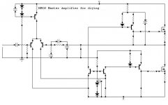
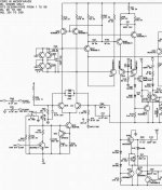
Workhorse said:hi every body,
here is a new update to the schematic with Push-pull drivers and optocoupled biasing with mosfet as thermal referencer.
Hm... way too complicated for my liking...
How about input PNP LTP feeding second stage NPN LTP connected to a PNP folded cascode driving the outputs directly?
2nd stage LTP and folded cascode terminate at the bootstrapped supply.
The disadvantage with this is increased losses in the driver stage as 2nd stage LTP and folded cascode spans ~full rail voltage and has to provide all the driving current since the folded cascode has no AC current gain.
Also reference voltage of the folded cascode terminates in the bootstrapped supply whic means you need to use a current source pull down for good PSRR.
Advantage is relatively easy biassing - provided Re of cascode is equal to Rgs of output MOSFETs, the reference voltage for the cascode bases equals bias Vgs + one diode drop. Also, current drain from bootstrapped supply is constant due to the differential action of the LTP/folded cascode. Finally, current limit is easy as maximum Vgs voltage swing is defined (Rgs * Itail of 2nd LTP at most).
For amplifierguru: don't worry, this is just a mental exercise 😉 at least for me...
Hi Kanwar
Why don't you join pnp driver directly with mosfet's source?
I think it could give better HF switching. What do you think?
And give 3rd diode (or use 1 LED) to prevent drivers from B-class working at HF. Remember that you need lower gate R now..
just suggestions...
regards
forgot to mention:
it would be easier to modify ref. voltage for folded cascode (from your post25) by Vgs multiplier except these diodes to keep bias steady.
Hi, Kanwar,
This could be a good design 😀
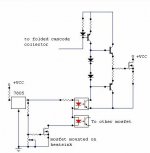
Here I attach a proposal for thermal compensation scheme, Q113 is attached to heatsink for thermal compensation.
Also the driver of the final NCH mosfets are totem-pole Q128-129 (biased with D110-111) and Q118-119 (biased with D107-108)
This could be a good design 😀
Here I attach a proposal for thermal compensation scheme, Q113 is attached to heatsink for thermal compensation.
Also the driver of the final NCH mosfets are totem-pole Q128-129 (biased with D110-111) and Q118-119 (biased with D107-108)
Attachments
Not that smart .....but
Hello Workhorse and others;
I'm not very smart and have trouble understanding how the bootstrap can overcome the minimum Vgs drive requirements of an N-channel output stage running off the positive rail.
Bootstraping if I understand correctly, is used to increase the open loop gain of an amplifier. So how is this related to the getting the amplifier to swing fully to rail?
An n-channel FET when driven off the positive rail can only swing to within the voltage differential between the gate and the source. So when the source (speaker out) approaches the positive rail voltage (or FETS drain voltage) less voltage is available to the gate.
Lets suppose a FET needs 4 volts gate-source to turn on and say 6 volts to deliver 10 amps, problems arise when the output swings to within Rail minus Vgs. So the amp appears to clip.
I thought the only way around this is too supply Rail Volts plus the required Vgs in order to provide enough voltage drive to the FET gate.......or
Have I missed something??
Cheers
Re: Not that smart .....but
Hi Quasi,
Bootstraping is used to boost the drive signal to get maximum swing. This is how it works.
in no signal conditions the cap will be charged at a refernce voltage between the resistor and output. When the lower mosfet starts conducting the the out put swings negative and then the Voltage across cap will be Vref+Vnegswing and then it gets charged to high voltage and again when positive signal appears, the the gate of mosfet sees an elevated voltage due to charge stored by cap and it gets an extra voltage at gate by the virtue of virtual supply emulated by the cap between resistor and output , thus the output swings to rail.
This technique is always used in Class-D drivers to get max High side mosfet swing.
hope you understand it.
quasi said:Hello Workhorse and others;
I'm not very smart and have trouble understanding how the bootstrap can overcome the minimum Vgs drive requirements of an N-channel output stage running off the positive rail.
Bootstraping if I understand correctly, is used to increase the open loop gain of an amplifier. So how is this related to the getting the amplifier to swing fully to rail?
An n-channel FET when driven off the positive rail can only swing to within the voltage differential between the gate and the source. So when the source (speaker out) approaches the positive rail voltage (or FETS drain voltage) less voltage is available to the gate.
Lets suppose a FET needs 4 volts gate-source to turn on and say 6 volts to deliver 10 amps, problems arise when the output swings to within Rail minus Vgs. So the amp appears to clip.
I thought the only way around this is too supply Rail Volts plus the required Vgs in order to provide enough voltage drive to the FET gate.......or
Have I missed something??
Cheers
Hi Quasi,
Bootstraping is used to boost the drive signal to get maximum swing. This is how it works.
in no signal conditions the cap will be charged at a refernce voltage between the resistor and output. When the lower mosfet starts conducting the the out put swings negative and then the Voltage across cap will be Vref+Vnegswing and then it gets charged to high voltage and again when positive signal appears, the the gate of mosfet sees an elevated voltage due to charge stored by cap and it gets an extra voltage at gate by the virtue of virtual supply emulated by the cap between resistor and output , thus the output swings to rail.
This technique is always used in Class-D drivers to get max High side mosfet swing.
hope you understand it.
ilimzn said:
Hm... way too complicated for my liking...
How about input PNP LTP feeding second stage NPN LTP connected to a PNP folded cascode driving the outputs directly?
2nd stage LTP and folded cascode terminate at the bootstrapped supply.
The disadvantage with this is increased losses in the driver stage as 2nd stage LTP and folded cascode spans ~full rail voltage and has to provide all the driving current since the folded cascode has no AC current gain.
Also reference voltage of the folded cascode terminates in the bootstrapped supply whic means you need to use a current source pull down for good PSRR.
Advantage is relatively easy biassing - provided Re of cascode is equal to Rgs of output MOSFETs, the reference voltage for the cascode bases equals bias Vgs + one diode drop. Also, current drain from bootstrapped supply is constant due to the differential action of the LTP/folded cascode. Finally, current limit is easy as maximum Vgs voltage swing is defined (Rgs * Itail of 2nd LTP at most).
For amplifierguru: don't worry, this is just a mental exercise 😉 at least for me...
I think this will simply increase something i dont like .......
darkfenriz said:Hi Kanwar
Why don't you join pnp driver directly with mosfet's source?
I think it could give better HF switching. What do you think?
And give 3rd diode (or use 1 LED) to prevent drivers from B-class working at HF. Remember that you need lower gate R now..
just suggestions...
regards
forgot to mention:
it would be easier to modify ref. voltage for folded cascode (from your post25) by Vgs multiplier except these diodes to keep bias steady.
The PNP driver will then has to be ascertained to deliver more current to charge the gate at high frequencies. Driver improve turn-off capability as well.
Regarding cascodes, shouldn't the VGS multiplier degrades its performance by changing it operating voltage thus current through it and eventually the voltage gain, if not then it will be very easy to implement it.
lumanauw said:Hi, Kanwar,
This could be a good design 😀
Here I attach a proposal for thermal compensation scheme, Q113 is attached to heatsink for thermal compensation.
Also the driver of the final NCH mosfets are totem-pole Q128-129 (biased with D110-111) and Q118-119 (biased with D107-108)
This is surely a complex thing not recommended for diying purposes. May i could give it a consideration too, but I am very busy right now.
regards,
Kanwar
Hi, Kanwar,
I think your design of full Nch+folded cascode could end up in a good DIY amp. Please keep up the good work 😀
I think your design of full Nch+folded cascode could end up in a good DIY amp. Please keep up the good work 😀
Sorry Kanwar
I wanted to ask you:
why don't you join pnp driver's COLLECTOR with mosfet's source?
this could change voltage drop on source resistor at HF.
I wanted to ask you:
why don't you join pnp driver's COLLECTOR with mosfet's source?
this could change voltage drop on source resistor at HF.
- Status
- Not open for further replies.
- Home
- Amplifiers
- Solid State
- NVMOS amplifier