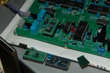
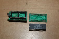
9001 to 8412 converter board completed.
One change is to add a 750ohm resistor (temporary leaded) at the pin 9 and 10 of the converter board, ie the input pins of the receiver IC 26C32 to move the DC voltage to about 2.5Vdc.
Listening test is underway.
One change is to add a 750ohm resistor (temporary leaded) at the pin 9 and 10 of the converter board, ie the input pins of the receiver IC 26C32 to move the DC voltage to about 2.5Vdc.
Listening test is underway.
Attachments
For the trial, I go back to single K170 for the input Jfet and also the lower current source back to 3.5mA (R3/R12 back to 33ohm). THat is the original design values and it gives me more sweetness on the music.
The ver3 board has been released to pcb factory and here are the changes relative to ver2.
1. Able to use DIR9001 daughter board upgrade beside 8414 daughter board.
2. Add one more K170 footprint on the input of Jfet IV so that two BL grade fets can be used instead of V grade K170 (can’t find).
3. Add one more pad for J74 current source in case J74V grade Idss 15mA fet is not found.
4. Enlarge pad sizes of passive parts like resistors, capacitors and inductors etc… on bottom size.
5. Increase pcb thickness to 2mm with gold plated through holes. White mask with black text.
6. Add more pitch size selection of output couple capacitor – 10uF (max 2 inches).
7. Add ground plan on the bottom size of digital section to improve grounding.
8. Add LM317 for pre-regulation for digital ICs and then LT1117-5V regulator for each digital IC.
9. Only use LM336-5V voltage reference at +/-18V low noise regulators in analogy supply.
10. Eliminate 90 deg turn on trace for digital signal paths.
11. Correct D10 polarity mark “+”.
12. Separate the digital supply of PCM63 from the analogy supply.
13. Two ground plans (D & A) and single point of connection at the centre location L21.
14. Add more via hole to improve the grounding at top and bottom ground plan of digital section.
15. Add ground points J19/J23/J24/J17/J26 so that diyer can add additional star ground if required.
16. Add TO-220 type fred diode pad for user upgrade.
17. All more pre-filtering capacitor pad.
18. Move the Jfet IV next to the current output of PCM63 to eliminate any noise pickup or leakage.
19. Add output relay for power off mute and power on delay.
20. Change analogy transformer from 24V x 2 to 18V x 2. Less heat on the low noise pre-regulator.
21. Add selection of 8412/14 output at 16 or 18 bit mode and also SM5842 input at 16 or 18bit mode.
22. Improve all pot tuning to clockwise direction for higher level or voltage etc…
23. Add jumper (or hard wire) for all LM317/337 regulators and thus easy to connect additional dc source for comparison.
24. One heat sink type – easy to source parts.


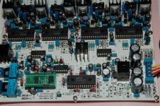
I have built two set with a bit different parts in the last 1.5 week and they are working fine. This kit is sure more difficult to build compare to ver2 due to very dense parts placement and more wirings for the PCM63 digital supply (either from analogy or digital side).
OK, the pcb/kit is ready to go! Here is thet BOM and pirce. The other files like schemetic/assembly instruction/pcb silkscreen top are too big to post here and I shall send to you when you order the kit.
Once again this is a project for experienced person and think twice before you order.
Picture will follows later as I am busy for work this week.
Enjoy.
Attachments
There will be some more delay on the D1V3 board release as I find some quality issue on the boards and I need to return to the pcb factory to perform a 100% open/short test. It will take about 2 more weeks time!
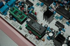
Here are two more photo on the two sets that I built so far. The one using normal E-cap parallel with film cap does not sound as good as the one that I use 18uF Rifa film cap. I added a shield on the 18uf film output so that there will be less interference among them to prevent any noise or even oscillation.
Here are two more photo on the two sets that I built so far. The one using normal E-cap parallel with film cap does not sound as good as the one that I use 18uF Rifa film cap. I added a shield on the 18uf film output so that there will be less interference among them to prevent any noise or even oscillation.
Attachments
I have started shipping some of the D1V3 boards but it is slow as the time to do kitting is not easy.
I have tried PCM63P-K2 on my DAC and the K2 chips sound more dynamics than the standard K version. Here is one picture of the chip. It is a used chip selling for US$35 per pc and is hard to find!
I shall contact those that have pre-order the pcb in the next 1~2 weeks.
I have tried PCM63P-K2 on my DAC and the K2 chips sound more dynamics than the standard K version. Here is one picture of the chip. It is a used chip selling for US$35 per pc and is hard to find!
I shall contact those that have pre-order the pcb in the next 1~2 weeks.
Attachments
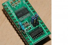
PMD100 converter board has been tested successfully in D1V3. Note that this board is only for D1V3 user.
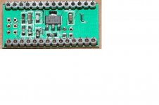
Bare PCB is US$5. $6 will include pcb x 1, pins x 2, 0.1uf x 2, resistor x 1, LED x 1, IC socket x 1.
I have some PMD100 chips (brand new never used) selling with the full kit for $30 to D1V3 diyer.
Spencer
Bare PCB is US$5. $6 will include pcb x 1, pins x 2, 0.1uf x 2, resistor x 1, LED x 1, IC socket x 1.
I have some PMD100 chips (brand new never used) selling with the full kit for $30 to D1V3 diyer.
Spencer
Attachments
- Home
- Vendor's Bazaar
- NP D1 DAC clone with enhancement