There may be many reasons as to why peppe sez he doesn’t have the means. I suggest we help him if he wants it real bad. You can ship that drek to me, or even better, to OPLDF. I hear he is two weeks on without constructing a new amp. Idle hands is never goodHave you tried building anything smd? If you have a magnifier and a fine soldering bit it's really not a problem. Just practice and find what works for you. I do the blob one pad - hold the part with tweezers - melt the blob - slide into place - solder the other pad method. I built a D3 no issues. Have a go!


Don't want to derail the thread but I meant what I said in an encouraging way. I think a lot of people are scared of smd because they think of terrifying robot pick and place machines, incomprehensible paste masks and ovens from Hades. They don't even consider it because it's scary... but the same rules apply, pad, component, solder. By hand is quite doable for an awful lot of smd packages. Try a practice kit, back to the topic and I'll shut up now 😊
Yep Simnon build a lot of tripath smd amp with just ....plus a lot of patient 😉

As above, but buy some solder paste - it's a game changer for smd.
OPLDF for sureThere may be many reasons as to why peppe sez he doesn’t have the means. I suggest we help him if he wants it real bad. You can ship that drek to me, or even better, to OPLDF. I hear he is two weeks on without constructing a new amp. Idle hands is never good
Et voilà, first questions for BOM:


Thanks in advance
- Are C27 and C28 necessary?
- All resistors 1/4W?
- Mosfet matched?
- Voltage (25-0-25 VAC?) and VA for donut?
- Heatsinks on 317s?
Thanks in advance
- start without them; if your dog or parrot leave a room, put something
-yup
-nope
-recalculate Vout of LM chips, then tell me, so I can tell you; have no notes and why should I for trivia
-nope
-yup
-nope
-recalculate Vout of LM chips, then tell me, so I can tell you; have no notes and why should I for trivia
-nope
consider this as a starting point:What do you think of that board as starting point?
https://a.aliexpress.com/_EQTXwGr
https://www.diyaudio.com/community/...s-input-nos-r-2r.354078/page-256#post-7128519
thanks!- start without them; if your dog or parrot leave a room, put something
-yup
-nope
-recalculate Vout of LM chips, then tell me, so I can tell you; have no notes and why should I for trivia
-nope
By Thorsten L. :As you said, the TDA1541A actually wants see a low impedance load for best performance.
The data sheet (page 7) says, "To ensure no performance losses, permitted output voltage compliance is ±25 mV maximum."
The current output of the chip is +/-2mA, with an offset of -2mA.
So for +/-25mV, maximum, the chip wants to see about 12 Ohm maximum. I'm sure that is why peppennino is interested in the D1's input impedance. 🙂
But then I load my dac with about 70R IV resistor and enjoy its sound. diyAudio member ecdesigns (John Brown), who has done a lot of work with the TDA1541A, has suggested that up to 150R may be used for IV.
ecdesigns IV resistor
But the D1 circuit is cool. The input mosfet is a current buffer. 🙂
I may try it but use a lower value for R4 since I don't need 3Vp output.
The Philips Datasheet is conservative. At AMR we did run extensive tests on that. The TDA1541 can handle more but not a LOT more. 50 Ohm I/V resistance is fine.
Secondly, if you want to stay within the 25mV compliance reliably for all possible output currents of the TDA1541 range you need 5.4 Ohm I/V conversion resistor (0.025V / 0.0046mA = 5.435Ohm).
My original "Adagio" DAC with TDA1541 used approximatly this value of resistance and a 1:15 Step Up Transformer. It also used an SRPP output stage tuned for lowest distortion, due to concerns about some of the ultrasonic "images" produced by the absence of oversampling folding back into the audio range.
Yes, I am aware of Thorsten Loesch's recommendations. Note that I currently use an I/V resistor of 70 Ohm.
My first TDA1541A dac that I built many years ago was based on Thorsten's first published TDA1541A dac, the Adagio, with SPDIF input and CS8412. I think I used an I/V resistor of about 20 or 25 Ohm and fed the output to a single ended 5842 output stage.
Years later I built another dac based on Thorsten's recommendations on this diyAudio thread: TDA1541A Veroboard dac
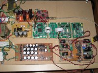
Later I deleted the on-board reclocker and divider and added IanCanada's isolator, FIFO, and clock. The first picture shows this setup with the Veroboard dac at the lower right of the picture.
RyanJ's D3 board is now used in place of the Veroboard dac, and I take I2S directly out from a single board computer to the FIFO and clock. I still use the power supplies on the Veroboard to power the I2S to simultaneous converter and to power some of the IanCanada boards. I/V is my own hand wound 70 Ohm resistors with my preamp providing voltage gain.
I think it sounds really good.🙂
My first TDA1541A dac that I built many years ago was based on Thorsten's first published TDA1541A dac, the Adagio, with SPDIF input and CS8412. I think I used an I/V resistor of about 20 or 25 Ohm and fed the output to a single ended 5842 output stage.
Years later I built another dac based on Thorsten's recommendations on this diyAudio thread: TDA1541A Veroboard dac
Later I deleted the on-board reclocker and divider and added IanCanada's isolator, FIFO, and clock. The first picture shows this setup with the Veroboard dac at the lower right of the picture.
RyanJ's D3 board is now used in place of the Veroboard dac, and I take I2S directly out from a single board computer to the FIFO and clock. I still use the power supplies on the Veroboard to power the I2S to simultaneous converter and to power some of the IanCanada boards. I/V is my own hand wound 70 Ohm resistors with my preamp providing voltage gain.
I think it sounds really good.🙂
Attachments

Circa 30V-recalculate Vout of LM chips, then tell me, so I can tell you; have no notes and why should I for trivia
nice me too long time on tda nos ,1543 on 2007 and AYAII from 2013Yes, I am aware of Thorsten Loesch's recommendations. Note that I currently use an I/V resistor of 70 Ohm.
My first TDA1541A dac that I built many years ago was based on Thorsten's first published TDA1541A dac, the Adagio, with SPDIF input and CS8412. I think I used an I/V resistor of about 20 or 25 Ohm and fed the output to a single ended 5842 output stage.
Years later I built another dac based on Thorsten's recommendations on this diyAudio thread: TDA1541A Veroboard dac
Later I deleted the on-board reclocker and divider and added IanCanada's isolator, FIFO, and clock. The first picture shows this setup with the Veroboard dac at the lower right of the picture.
RyanJ's D3 board is now used in place of the Veroboard dac, and I take I2S directly out from a single board computer to the FIFO and clock. I still use the power supplies on the Veroboard to power the I2S to simultaneous converter and to power some of the IanCanada boards. I/V is my own hand wound 70 Ohm resistors with my preamp providing voltage gain.
I think it sounds really good.🙂
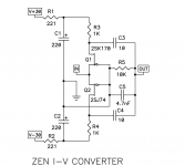
Circa 30V
so current in each first section is neg 30V/string of source resistors
that would be 30V/3K3=9.1mA
buffer Iq is - voltage at gate (30V-(9.1mA*R4 deduct 4V)), divide with 1K5 = 8.2mA
gives sum of, say, 18mA per side
36mA entire shebang
xformer at least 56V center-tapped - try to find adequate close standard one
56Vac * 36mA gives 2VA
so 10VA Donut logical choice ........ of course you can use more
- Home
- Amplifiers
- Pass Labs
- NOS TDA1541 + D1 I/V & output stage