I know from earlier (when Quasi was more active on this site) that he was/is a very kind, honest and helpful person. I highly doubt that he put out something that doesn't work. I just had some questions.
Layout design is for sure an interresting subject.
To pickup something from an antenna you need a transmitter. What is transmitting close to your supposed antennas? How will the oscillating feedback form? Further, in an opamp you are dealing with the whole amp not a part of it.
Layout design is for sure an interresting subject.
To pickup something from an antenna you need a transmitter. What is transmitting close to your supposed antennas? How will the oscillating feedback form? Further, in an opamp you are dealing with the whole amp not a part of it.
Ok, you try to help me, but I dont know how to do that 🙁. There are 100nF capacitors from positive end negative rail to GND just to the right of small common heat sink.
Quasi was a good guy and very patient ,as well. I learned more discussing the basic "blameless" (nmos 200/350) on his thread than reading self's book !
Reading and participating in that thread , there were PCB layout "bugs" discussed. One was in the vbe. Some builders DID experience oscillation (it's in the thread).
I used larger gatestoppers and ferrite beads on the MOSFETS in my attempt to make a simple Nmos 200. It worked well , but lacked the sound quality for a full range amplifier.
The amplifier in general is of sound design , but not refined. What I mean is : no beta enhancement on the VAS , the Vbe wiper could fail and fry the amp , very basic current sources with less than optimum rail conditioning. (plus- no gate protection , ferrite beads for safety , per device OP decoupling - all V mosfet specific)
Just as an example of before and after (pix 1 and 2) I started with quasi's nmos 200 and ended with mine 2 years later. 🙂
PS , V mosfets will oscillate in the 30-50mhz range , much higher than a cheap CRO will "see" , the beads and larger gatestoppers will negate this. My opinion is that V mosfets are "more ideal" for switching and PS's , not linear audio. I use BJT and Lfets exclusively !
OS
Attachments
Last edited:
Hello ID_ (and friends)
It seems that you have a genuine fault that you may not have found yet. When fault finding or testing the amp I suggest you do so with 100 ohm resistors in place of the fuses, you may not be able to fully set the bias current but you will be able to fault find the amp without destroying the output FETs. Once you have found the fault you will need to go through the full setup procedure again.
There have been hundreds of these modules built (maybe over a thousand) so I'll run through the more common problems and recommendations.
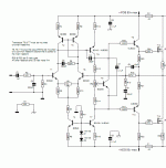
- The 0.1uF decoupling capacitors near the input stage (next to the small heatsink) must be poly types or similar as to avoid power supply oscillations. Under no circumstances should you use ceramic types here. There must be 0.1uF poly capacitors at other decoupling locations ie; near the fuses and across the main power supply caps.
- Transistor T8 is shown mirror image on the PCB because it mounts underneath so make sure you have the pin-outs correct. This could explain the thermal runaway.
- Some constructors forgot to install the ground link underneath the board. This link is absolutely necessary and presents no risk of oscillation in this application, provided that other good chassis wiring is adhered to. Running parallel to the output track is fine at this signal level.
- About the most common fault is incorrect component (especially resistors that can be hard to read). One constructor built a perfectly good amp with a gain of 3. I thought it was funny anyway.
- Bad PCB tracks with minute (invisible) fractures have also made it to the list.
- Next is punctured isolation pads for the relevant mosfets and transistors. You must check for shorts between the heatsinks and the semiconductors every time you mount or remount them. This would explain some of the wierdest faults I have found.
- The main heatsink (the one the mosfets mount on) must be grounded to 0v either via the main chassis or via a lead during testing. Whilst I have not experienced it there is a potential for wierd capacitive effects to be present. Grounding the heatsink swamps these out. You can also ground the small heatsink too if your nervous about strong noise fields.
- There is no risk of thermal runaway in the second and third stages. The second feeds off a constant current source and this controls the 3rd stage.
- Component quality is important, I have had reports of constructors changing the brand of a component and solving a problem.
- The problem of the bias control is known and resolved by linking the wiper to the 47 ohm resistor - trimmer pot junction. If the wiper goes open you will lose output bias but that's about it.
- About your own amp, if you are getting thermal runaway then there is something wrong with the Vbe section of your amp. It could be that T8 is faulty or it's pinouts are wrong. It is also possible that you have a fault in the 2nd or 3rd stage as well that is somehow affecting this.
- I doubt the noise you heard is an oscillation associated with poor amp design, this would likely be way outside the audio spectrum so what you heard probably had something to do with the original fault.
- The heatsink for the second and third stages will run hot (especially with 81v rails), this is normal and the transistors specified can take it.
That's it from me for now, if you post some detailed photos of your build maybe I (and others) can offer more help. I'm not on as often as I used to be but happy to help where I can.
Cheers
Quasi
It seems that you have a genuine fault that you may not have found yet. When fault finding or testing the amp I suggest you do so with 100 ohm resistors in place of the fuses, you may not be able to fully set the bias current but you will be able to fault find the amp without destroying the output FETs. Once you have found the fault you will need to go through the full setup procedure again.
There have been hundreds of these modules built (maybe over a thousand) so I'll run through the more common problems and recommendations.
- The 0.1uF decoupling capacitors near the input stage (next to the small heatsink) must be poly types or similar as to avoid power supply oscillations. Under no circumstances should you use ceramic types here. There must be 0.1uF poly capacitors at other decoupling locations ie; near the fuses and across the main power supply caps.
- Transistor T8 is shown mirror image on the PCB because it mounts underneath so make sure you have the pin-outs correct. This could explain the thermal runaway.
- Some constructors forgot to install the ground link underneath the board. This link is absolutely necessary and presents no risk of oscillation in this application, provided that other good chassis wiring is adhered to. Running parallel to the output track is fine at this signal level.
- About the most common fault is incorrect component (especially resistors that can be hard to read). One constructor built a perfectly good amp with a gain of 3. I thought it was funny anyway.
- Bad PCB tracks with minute (invisible) fractures have also made it to the list.
- Next is punctured isolation pads for the relevant mosfets and transistors. You must check for shorts between the heatsinks and the semiconductors every time you mount or remount them. This would explain some of the wierdest faults I have found.
- The main heatsink (the one the mosfets mount on) must be grounded to 0v either via the main chassis or via a lead during testing. Whilst I have not experienced it there is a potential for wierd capacitive effects to be present. Grounding the heatsink swamps these out. You can also ground the small heatsink too if your nervous about strong noise fields.
- There is no risk of thermal runaway in the second and third stages. The second feeds off a constant current source and this controls the 3rd stage.
- Component quality is important, I have had reports of constructors changing the brand of a component and solving a problem.
- The problem of the bias control is known and resolved by linking the wiper to the 47 ohm resistor - trimmer pot junction. If the wiper goes open you will lose output bias but that's about it.
- About your own amp, if you are getting thermal runaway then there is something wrong with the Vbe section of your amp. It could be that T8 is faulty or it's pinouts are wrong. It is also possible that you have a fault in the 2nd or 3rd stage as well that is somehow affecting this.
- I doubt the noise you heard is an oscillation associated with poor amp design, this would likely be way outside the audio spectrum so what you heard probably had something to do with the original fault.
- The heatsink for the second and third stages will run hot (especially with 81v rails), this is normal and the transistors specified can take it.
That's it from me for now, if you post some detailed photos of your build maybe I (and others) can offer more help. I'm not on as often as I used to be but happy to help where I can.
Cheers
Quasi
Hello Quasi.
Thank's that you responded to my problem!
I checked and rechecked all the tracks on PCB and all components. The only difference to the original I made is that I changed T1 and T5 (2sc1845) to 2sc2240, becouse I couldn't get them and instead of 200 ohm (VR2) I instaled the 220 Ohm.
All 100nF capacitors are poly type.
I checked for the contacts of semiconductors to the main heat sink and there is no contact. T6, 7, 9 and 10 have also no contact with the small common heat sink.
T8 is mounted right way (as pictured on the layout).
As everything seems to be ok, I connected the amp to the PSU with 100ohm resistors in place. When I turn the trimm pot VR2 fully clockwise I get about 12V across the 100 Ohm resistor in positive rail. But as I do this, the small common heat sink gets extremely hot and the voltage (current) across 100 ohm resistor is rising untill the temperature settles. I can set the biass only in last 1/3 as I turn the VR2. This is strange to me and I asume, something must be wrong here but I can't find out what. The main heat sink remains cold!
I haven't grounded either main or small heat sink.
When I first connected the amp the long ground wire link vas underneath the PCB. I thought this might be a problem and I moved the link to the top side. This didn't solved the problem.
I've made now some scope testing. The whole thing is oscilatin like crazy!
This is the input pin.
This is the input ground pin
If I ground the small common heat sink I get these resoults:
Inpit ground pin
Input pin
But it gets extremely hot anyway!
And the amp on the large heat sink wich remains cold (I'll replace it with another, when I'll put the amp in housing)
Iff I ground the large heat sink there is no diference.
An externally hosted image should be here but it was not working when we last tested it.
This is the input pin.
An externally hosted image should be here but it was not working when we last tested it.
This is the input ground pin
If I ground the small common heat sink I get these resoults:
An externally hosted image should be here but it was not working when we last tested it.
Inpit ground pin
An externally hosted image should be here but it was not working when we last tested it.
Input pin
But it gets extremely hot anyway!
And the amp on the large heat sink wich remains cold (I'll replace it with another, when I'll put the amp in housing)
An externally hosted image should be here but it was not working when we last tested it.
Iff I ground the large heat sink there is no diference.
Your scope is awfully dirty and dusty😛😉
Do you have a 100-220pF capacitor between B and E on VAS ? If not, try it, it might help.
100pF between B and C of the drivers might also help.
Do you have a 100-220pF capacitor between B and E on VAS ? If not, try it, it might help.
100pF between B and C of the drivers might also help.
What is the current running through r20 ? can you measure about 18 mV as specified in the schematics ? Look at the voltage across r20, while quiescent, using a scope, are there oscillations ?
I set the quiescent current to the max- I get reading of 12,45V across the 100 Ohm resistor in positive rail-->24mA per FET pair. Then in measured voltage across the resistor R20. I get 3,45V-->15mA.
So this is OK.
Then I looked for oscilations with scope (connected the ground of probe to ground on amp and tip to the R20). There are oscilations. I can see nice sine wave!
@Tekko
Wich transistor are VAS?
So this is OK.
Then I looked for oscilations with scope (connected the ground of probe to ground on amp and tip to the R20). There are oscilations. I can see nice sine wave!
@Tekko
Wich transistor are VAS?
I am not really sure how you measured your currents, but I assume its OK.
At what frequency are the oscillations you can see with the scope ?
Do the oscillations seem to appear in only one frequency ?
What amplitude do they have ?
At what frequency are the oscillations you can see with the scope ?
Do the oscillations seem to appear in only one frequency ?
What amplitude do they have ?
I measured the voltage drop across the resistor R20. It gives me reading of 3,45V. So the resistor is 220 Ohm--> 3,45V/220Ohm=15,68mA.
The oscilation appears at about 3MHz with amplitude of about 55mV p-p.
The oscilation appears at about 3MHz with amplitude of about 55mV p-p.
VAS or voltage amplification stage is the reansistor whose collector connects to the bias transistors collector and the upper driver transistors base.
The oscillations are the reason for heat, because the VAS must work as hell. I wonder why the great heatsink not hot as well. This isn't a good sign. 🙁
Please measure the output of this amp.
Do you decoupled the diff-amp how I told?
Please measure the output of this amp.
Do you decoupled the diff-amp how I told?
I decoupled the diff-amp as you told me to. No change in in oscilation when I did that. In output I get the same oscilation as in R20 (about 3MHz and about 70mV p-p). I can trimm the DC ofset with VR1 to almost 0mV and it stays there.
I'll give it a try and put 150pF ceramic capacitor between B and E of T6.
I'll give it a try and put 150pF ceramic capacitor between B and E of T6.
I decoupled the diff-amp as you told me to.
🙂 very nice
In output I get the same oscilation as in R20 (about 3MHz and about 70mV p-p)
nice too...so far
I'll give it a try and put 150pF ceramic capacitor between B and E of T6.
That should help, but it is verv much.
Often make C8 problems, when it isn't correct tuned, then it does the opposite that it should.
Try to remove it and measure.
If I remove the C8 (10pF) the oscilation frequency lowers to 50Hz (pure sine wave can be seen!) and amlitude gets to approx. 160mV p-p
If I remove the C8 (10pF) the oscilation frequency lowers to 50Hz
So far, so good. 🙂
50Hz sounds like grounding-hum...next problem 😛
But again to the oscillation C3 with 330p seems to be to small, I would take 2200p. C3/R9 reduce the open-loop bandwidth.
Interesting!!
When I changed the C3 (330pF) to 2,2nF all I can se on the scope is straight 0V line in the middle of the crt screen! No sign of any oscilation! I probed the input pin and input ground pin, R20, R25 and output- an all pins there is straight line! I tried to touch the input pin when I probed the output pin and it responded to the touch. As I removed finger, the output went back to 0V straight line.
Now im tempted to connect the speaker, but I'm afraid something would go wrong! Any chance to connect the speaker the way I don't blow the amp!?
I dont own the variac 🙁
do not connect a speaker, instead connect a resistive dummy load.
Short the input temporarily, while you take measurements.
When you have all the voltage measurements and from there all the current flows you can post details on a schematic.
Then the fault finding experts on the Forum can try to trace what fault is causing this oscillation problem. Once that is sorted then you can progress to finding the optimum stability compensation, before you even think about attaching a speaker.
- Home
- Amplifiers
- Solid State
- NMOS 350/500 by Quasi