Neither. You want to take the feedback after the emitter currents have summed. This means you need to take the feedback from the connection to the speaker.
Douglas Self has written quite a bit about this. You can find his thoughts in his papers from Wireless World in the mid/late 1990s (and subsequent books).
Tom
Douglas Self has written quite a bit about this. You can find his thoughts in his papers from Wireless World in the mid/late 1990s (and subsequent books).
Tom

Its good to have a short section of trace between the summing point and the speaker connection, rather than sum at the speaker connection, since then the feedback pick-off point can be the other side of the speaker connection and be completely free of non-linear currents (each emitter carries half-cycles which are extremely distorted).
Its good to derive the ground for the input section from a point close to the speaker cold terminal (although ground currents are linear in the output section, some non-linearity is injected from the decoupling caps and the same principle applies although much less severe.
A one inch section of trace that's 1/4 inch wide has a resistance of 2 milliohms for standard PCB, 2 milliohms is 1/4000th of the 8ohm load, so non linearity of current in that section is reduced by 72dB (voltage divider effect). Say single rail current is 30% THD (a guess), that means such a short trace could inject upto -80dB THD purely through a sub-optimal layout (greater for a 4 ohm load).
To be clear in actual operation the feedback pick-off point is the point where the distortion will be minimized, so place it at the speaker connection or if not, ensure the trace between the speaker connection and pick-off point only carries linear current.
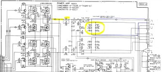
https://www.diyaudio.com/community/attachments/maplin1-png.976806/
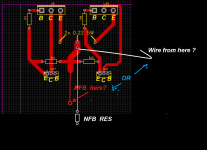
Is this a good example for the nfb trace routing?
Is this a good example for the nfb trace routing?
@Mark Tillotson Thank you, I'll modify and post here to ask if it's ok.
One discrete amp I've built before I did it like post 1 red trace "without problems " , another time I did , if I touched the speaker terminals on the speaker itself I could hear a buzz coming from my finger as if I touched the input. So definitely not good.
Didn't had the issue with ic amps , as traces were very close to the ic itself .
And the input/NFB/speaker grounds tie at a single point, isolated from other stuff. Then both channels tie together, then return to the power supply ground (With all the stuff like zobels, protection, bypassing, etc). If there are grounds that contain mostly linear signals internal to the feedback (ie degeneration), those tie together separately and then return to power supply ground. Should look more like a little tree than one big star with too many things trying to run into exactly one point. If that “point” gets big and spread out enough it defeats its original purpose, which is keeping nonlinear voltage drops out of the path of linear ones. Parallel traces and ground lines longer than they need to be can cause unwanted couplings too. Don’t run the NFB path or linear ground returns in parallel with the lines that feed the output tranny collectors. Run them at right angles to one another if they have to cross.
Sorry. I didn't realize what I wrote could be understood the way it was. Here's what I meant:

And please kill the star ground. Just pour a ground plane on one layer and have a small ground pour on the other layer for the few nodes that need to connect to a quiet ground.
I really appreciate that you start the layout review process early. Good on you!
Tom
And please kill the star ground. Just pour a ground plane on one layer and have a small ground pour on the other layer for the few nodes that need to connect to a quiet ground.
I really appreciate that you start the layout review process early. Good on you!
Tom
Oh, Now i just saw the reply ! , So ground plane then ?.Sorry. I didn't realize what I wrote could be understood the way it was. Here's what I meant:
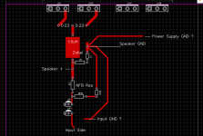
View attachment 1260159
And please kill the star ground. Just pour a ground plane on one layer and have a small ground pour on the other layer for the few nodes that need to connect to a quiet ground.
I really appreciate that you start the layout review process early. Good on you!
Tom
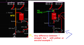
also any difference between straight line or like ur post.
Attachments
Resistor Cap network before the inductor ? or You mean the resistor inside the inductor ( inductor " winding on the resistor ?.You want the Zobel connecting on the 'inside' of the inductor.
Tom
Zobel network is before the inductor so that the amp can see it at high frequency, thus preventing the output stage being inductively loaded at VHF frequencies and oscillating.
Why did they do it the other way ? Pioneer amp .Zobel network is before the inductor so that the amp can see it at high frequency, thus preventing the output stage being inductively loaded at VHF frequencies and oscillating.
Attachments
Because they screwed up or didn't know better? They also have 100 Ω in parallel with the inductor in the Thiele network. That'll do absolutely nothing.Why did they do it the other way ?
The point of the Zobel network (R+C to ground) is to present a low-ish load on the amplifier at HF. The inductor presents a high impedance at HF so for the Zobel network to be effective it needs to be on the 'inside' of the inductor. You could argue that if you use a low resistance (say a few ohm) in parallel with the inductor you still get a low-impedance load at the amp at HF, but with the 100 Ω in the Pioneer or 10 Ω commonly used the Zobel is not that effective.
Yes. Ground plane. I don't understand the second part of your question. The point of a ground plane is to reduce impedance. Lower impedance -> lower error signal from the currents flowing in the plane.So ground plane then ?.
also any difference between straight line or like ur post.
Tom
@tomchr ok thank you !. so even 10 ohm is small? I need to read more on it. In simulations a 50Khz square wave was " more square" with the 100ohm resistor and 1.5uH inductor , then 10ohm res and 1.5uH inductor.
Also for NFB, 4700 and 220 ohm resistors 21.36 +1 , aroound 22gain , are the values to low? lower values less noise ?. I don;'t see the base of the LTP having more current drawn by it compared to using 21k and 1k .
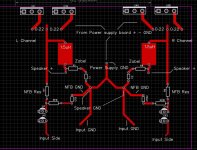
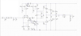
Here's my schematic .
Also for NFB, 4700 and 220 ohm resistors 21.36 +1 , aroound 22gain , are the values to low? lower values less noise ?. I don;'t see the base of the LTP having more current drawn by it compared to using 21k and 1k .
Here's my schematic .
Attachments
You can answer those questions by playing with the circuit in the simulator. Look at the noise performance and see if it changes appreciably as you change the impedance of the feedback network. I don't know what your design target is so I can't really provide a meaningful answer.
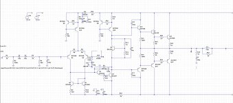
Depending on how powerful this amp is you may have to watch the power dissipation in R13.
Tom
Depending on how powerful this amp is you may have to watch the power dissipation in R13.
Yep.emitter into resistors togheter , wire for nfb, , then zobel , inductor , speaker.
Tom
- Home
- Amplifiers
- Solid State
- NFB Trace on PCB?