If at some moment you end up having your layout looking 99% like Tom's I would suggest to buy his PCBs instead of copying them😉
I started this thread as a learning exercise, it would have been a lot cheaper (in money and time) to buy Tom's board... however I wouldn't have learned as much as I have done. My PCB won't be as good as Tom's, but I will have built it myself and I will have learned a lot in doing so. I can measure the performance and work on improvements - that's what DIY is about isn't it?
Agree, I just suggested looking at Tom's layout if you are in doubt what clearance to take. My comment on copying is probably inappropriate. I apologise for it.
Agree, I just suggested looking at Tom's layout if you are in doubt what clearance to take. My comment on copying is probably inappropriate. I apologise for it.
No problem, I appreciate your advice so far.
As it is now your layout looks good as Tom already mentioned. Now you can start beautifying it🙂
Thanks all for your help again.
I'm finding that I need to read things through about six times before they start to sink
Simon.
This is how learning works for me, it took me a while to learn some of the methods here, often by asking questions here and the patience of members. The evidence is dotted around this forum 😀
I started this thread as a learning exercise, it would have been a lot cheaper (in money and time) to buy Tom's board... however I wouldn't have learned as much as I have done. My PCB won't be as good as Tom's, but I will have built it myself and I will have learned a lot in doing so.
As I've poured quite a bit of time into this thread, I did consider how much I should share. It would have saved me a lot of time to just post my layout and move away, but it wouldn't explain why I designed the board the way I did, thus wouldn't have resulted in the same learning experience. I'm also running a business and just giving away my products for free is not a viable business model. That said, I do enjoy teaching and do want to make a contribution to the DIY Audio community, so I chose to participate. I've had fun so far. It's always enjoyable to teach someone who wants to learn and is who able to follow directions.
One way I can leverage my contribution here in a more "business" sense is to include a link to this thread on my Taming the LM3886 pages. My goal with that would be to show how a decent layout can be done and also show that developing a decent layout actually takes some thought, knowledge, and real work. Perhaps for someone else that'll result in a similar learning experience or in the forking over of cash for one of my boards. After all, the PCB is only a small part of what I deliver. With the purchase of my LM3886DR you get 30+ pages of design documentation, including advice on the sizing of the power supply and heat sink, as well as a full set of measurements of the implemented circuit. You also get technical support should you get stuck.
Agree, I just suggested looking at Tom's layout if you are in doubt what clearance to take. My comment on copying is probably inappropriate. I apologise for it.
I'm glad you brought it up actually. No offence taken on my part.
Tom
I regretted about my suggestion to look at your layout shortly after I posted it. Knowing that you make a living with your diy oriented business I really think that you share a lot if not too much in view of your IP protection and I felt like I didn't help it by my comment, thus the follow up on copying. I really appreciate your contributions and learn a lot from your posts around the forum and I hope you'll continue sharing your knowledge with us.
Regards,
Oleg
Regards,
Oleg
I trust that there is an integrity check in the PCB program, it should complain profusely about the gaps between pads and areas as well as pads and tracks. I see short circuits between tracks and pours, unless the converting to a picture is really bad.
Goodluck
Goodluck
I'm sure there are minimum specified gaps between the traces, pads and pours in OP's layout. Eagle's image export algorithm is really bad. I usually use external gerber viewer to get better images of the layout. But checking if all is correct with the layout is advisable. Just use ERC and DRC tools to report schematic and layout errors.
I regretted about my suggestion to look at your layout shortly after I posted it. Knowing that you make a living with your diy oriented business I really think that you share a lot if not too much in view of your IP protection and I felt like I didn't help it by my comment, thus the follow up on copying.
I appreciate your concern. Yeah... My business started sorta by accident as a self-sustaining hobby. I keep edging closer and closer to a more "business" mindset. There is definitely a balance between sharing and keeping my IP to myself.
I really appreciate your contributions and learn a lot from your posts around the forum and I hope you'll continue sharing your knowledge with us.
You're welcome. I have no plans for going away so I'll stick around and help out here as long as I have time to do so. Given that DIY Audio is my favourite procrastination activity, I'm likely to stay active here for some time to come.
I'm sure there are minimum specified gaps between the traces, pads and pours in OP's layout. Eagle's image export algorithm is really bad. I usually use external gerber viewer to get better images of the layout. But checking if all is correct with the layout is advisable. Just use ERC and DRC tools to report schematic and layout errors.
I haven't used Eagle but every other tool I've used have supported DRCs. Usually the tool won't even allow you to draw something that violates the design rules. Now, this does require that the DRCs (mainly the trace/space widths) are set up correctly and the DRC feature is turned on, but that's pretty straight forward.
Running a Design Rule Check (DRC) once the layout is done is definitely required. I've also learned the hard way that generating a report of any unconnected nets can be valuable. Now I just include that check as part of my "tapeout" flow.
Tom
I've hit that order button for the PCBs so thanks again to everyone who's contributed and especially Tom for being so generous with his advice. I've learned more than I could have hoped and really enjoyed the process... I'm beginning to think I might have a half decent amp at the end of this and I didn't expect that! As I said before, if my primary interest was getting the best performance out of a chipamp then I would have ordered a set of boards from Tom in the first place.
I ran a DRC before posting most of the images here - as good as Eagle is it does produce crappy graphics. I resorted to screen-shots in the end.
Just need to put the boards together next...
Thanks again,
Simon.
I ran a DRC before posting most of the images here - as good as Eagle is it does produce crappy graphics. I resorted to screen-shots in the end.
Just need to put the boards together next...
Thanks again,
Simon.
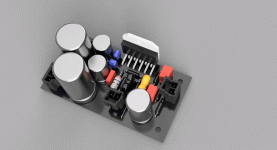
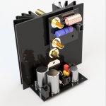
What do you do when you're waiting for your boards to arrive from China. Well if you're as anally retentive as me then creating a virtual version is a possibility. I need the dimensions to design the chassis, but couldn't help putting in a little bit extra detail.
Attachments
I'm not sure of the protocol here... if I should start a new thread to ask questions about the build someone tell me and I'll kill this one off.
Anyway, I've been working on a design for the amp and came up with the idea of making a kind of sub-assembly as shown in the pics; with the amplifier board, rca input and binding posts all attached to the heatsink.
I over-specced the heatsink so I don't think the extra holes are going to cause a problem, other than that does anyone foresee a problem with this design?
Before anyone asks if that's a suppository on the Thiele network, I know that resistor is a bit big. Also don't be fooled by the slick CAD, once I've got my greasy hands on the components the final product will look as though it's been run over by a bus.
Attachments
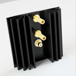
Over-specced the heat sink? It looks kinda small to me. Of course, this depends on your supply voltage. What thermal resistance is it specified at?
Tom
Tom
I've just re-done my calcs, I work out max power dissipation as 35.9W and I've got the insulated version of the IC so I need <1.3C/W... so looks like you're right - I need to find a bigger heatsink. I think I can get a taller one... does the premise of the idea cause any problems?
That'll work well if you're driving 8 Ω speakers. For 4 Ω, I recommend ±28 V. See my latest addition to the Taming series, Output Power.
Tom
Tom
- Status
- Not open for further replies.
- Home
- Amplifiers
- Chip Amps
- Newbie LM3886 Circuit