I suggest you swap the Spkr Return/gnd for the two HF decoupling caps.
That gets the HF decoupling route closer to the power pins.
Then move R7 to the right to create a bit of empty space.
Now move C12 down towards that empty space to bring the C12 route closer again to the power pin.
Now move C9 close to C12 and then rotate it 90degrees to bring the top lead very close to the power pin.
It's the length of the route and the area enclosed within the route that determines the impedance (mostly inductive at the frequencies where the HF decoupling is effective).
The total length of the route from the +pin through the two decoupling caps back to the -pin is important. The connection between the two caps becomes the HF audio and power ground.
A short link/plane to the MF power ground then finishes that bit of the layout.
For minimum impedance the speaker return should connect into that short link. Then at some middling frequency the two HF and MF routes will have similar impedances and thus present a roughly halved impedance to the speaker current flow. This is where the swappped location of the speaker return ends up BETWEEN the HF and MF power grounds and that (on a mono implementation) becomes the Main Audio Ground (MAG).
In a stereo implementation the MAG usually ends up off the PCB.
Last edited:
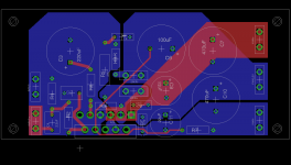
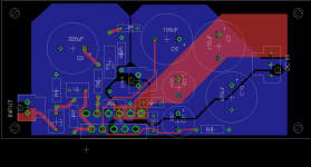
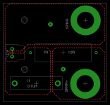
Some suggestions for improvement on the layout in Post #39:
I suggest reducing HBR to 0 Ω and swapping it and C4 in the layout. That'll bring the GND reference closer to the speaker ground terminal, thus reducing any error voltage there.
The node you have labeled as MAG (I'm assuming you mean Main Audio Ground) is actually not the main audio ground. The speaker ground terminal is. I suggest having a look at the Grounding Section of my Taming the LM3886 article series. I explain my reasoning there and back it up with simulation results. I also explains how the LM3886 uses the GND terminal.
R5 needs to be a 2 W type. I don't think that'll fit on your current footprint.
I'd bring C8 closer to the action. There's no reason not to and it will provide better decoupling.
I'd beef up the PWR+ connection. The board cost will be the same regardless of how much of the copper you use, so why not get your money's worth and improve the PSRR+ as well?
Tom
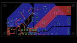
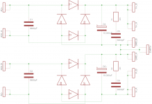
Thanks everyone for your continued help and patience. I've updated the layout to address your comments (hopefully I understood them). I've also included the schematic and layout for the power supply; I'm going to be using a 2x25V 300VA toroidal transformer.
Thanks, I'd changed the resistor power rating but forgot to update the footprint.
Sorry if this is a basic question, I'd never heard of a 0 Ohm resistor - does this mean it can just be a trace? Having just looked it up I now know you can buy the component, I just don't understand what that would do which would be different to a trace / jumper.
Thanks again for the help,
Simon.
R5 needs to be a 2 W type. I don't think that'll fit on your current footprint.
Thanks, I'd changed the resistor power rating but forgot to update the footprint.
I suggest reducing HBR to 0 Ω and swapping it and C4 in the layout.
Sorry if this is a basic question, I'd never heard of a 0 Ohm resistor - does this mean it can just be a trace? Having just looked it up I now know you can buy the component, I just don't understand what that would do which would be different to a trace / jumper.
Thanks again for the help,
Simon.
Attachments
C9 and C12 are normally 100nF. You can increase them to 220nF, if you can keep to the small package.
I can't see how you can get 4u7F into that small a package.
HBR can be a 0r0 link or a trace between two pads that can be cut later, or an actual resistor.
Leaving provision for HBR if required is a wise move in my book.
C2 is enormous. Why? 680pF is available as an MKP in 0.2" pin pitch.
C5 can be sqeezed down to 0.2".
I do recommend that you allow for pin pitch options for your smaller capacitors.
You often don't have the exact pin pitch in stock and it costs lots to order an exact size from a supplier. And some suppliers don't stock all the alternative pin pitch in the values you need.
options for 0.2", 0.3" & 0.4" are useful. & maybe 0.1" if you intend using tiny ceramic (which can be used for 805 smd caps).
If you intend using 1/4" spade for your power connectors, then place solder pads on both sides to strengthen the soldered connection.
I would not bother with thermal reliefs around spade solder pads. You put lots of heat into the spade and then solder the full pad.
Last edited:
C9 and C12 are normally 100nF. You can increase them to 220nF, if you can keep to the small package.
I can't see how you can get 4u7F into that small a package.
HBR can be a 0r0 link or a trace between two pads that can be cut later, or an actual resistor.
Leaving provision for HBR if required is a wise move in my book.
C2 is enormous. Why? 680pF is available as an MKP in 0.2" pin pitch.
If you intend using 1/4" spade for your power connectors, then place solder pads on both sides to strengthen the soldered connection.
The 4u7F is an x7r ceramic - do you think I should change this component?
I'll leave the HBR in the layout and experiment with jumper / resistor when I've assembled the board.
The component I was planning to use for C2 is this silver mica, do you think an MKP would be a better choice?
Thanks,
Simon.
The power supply smoothing capacitors are far too small
I was worried about that... from what I've read I can either go for lower value capacitors (albeit with easy to drive speakers) or go for a snubberised circuit with 10,000uF caps. After looking at the price of big caps, and considering I'm yet to build the speakers I'm planning on using with this amp I thought I'd start small and build efficient speakers then upgrade later if I need to. Does that sound like a good plan?
The layout is starting to look a lot better.
A few things you could still try:
Rotate both SPKR+ and -. Move HBR to the left of SPKR-. Move R5 and C4 to the right of SPKR+-.
Place C5 on the underside of the board between pins 9 and 10. This will give you more room to optimise the layout of the existing input parts.
Extend the input- plane to go under C2, R2, pins 7, 8, 9 and 10.
I have heard of using low value caps with "gainclones", to be honest, I don't get it. These aren't expensive and they're very good SLPX472M050A7P3 | Cornell-Dubilier Aluminium Electrolytic Capacitor 4700μF 50 V dc 22mm Through Hole A7 SLPX Series Lifetime 3000h +85degC | Cornell-Dubilier
or these SLPX103M050E7P3 | Cornell-Dubilier Aluminium Electrolytic Capacitor 10000μF 50 V dc 30mm Through Hole E7 SLPX Series Lifetime 3000h +85degC | Cornell-Dubilier
or these SLPX103M050E7P3 | Cornell-Dubilier Aluminium Electrolytic Capacitor 10000μF 50 V dc 30mm Through Hole E7 SLPX Series Lifetime 3000h +85degC | Cornell-Dubilier
Last edited:
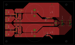
Thanks again everyone, here's the latest version of the amp layout.
C2 changed from Silver Mica to MKP to reduce footprint.
C5 (220pF) removed from layout, to be soldered directly onto the underside of the LM3886 input pins.
HBR & Speaker terminals re-orientated.
Signal return plane extended.
I'm trying to find a way of adding pads to the top layer under the spade terminals to add mechanical support... Eagle keeps accusing me of layer abuse when I try to do this.
scottjoplin - those capacitors look good value, I'll have a go at changing the power supply to a snubberised version.
Simon.
Attachments
The schematic looks ok but you've connected the 0V all the way through to the bridges on the layout, it would be better if they were connected at the output as in the schematic
Sorry if this is a basic question, I'd never heard of a 0 Ohm resistor - does this mean it can just be a trace?
You can actually buy 0 Ω resistors. You can also just use a piece of component lead clipping or wire. A trace will work too, but depending on your layout software you may need a node-breaker as you'll be trying to connect two different net names with a trace and the layout tool won't like that much.
C9 and C12 are normally 100nF. You can increase them to 220nF, if you can keep to the small package.
I can't see how you can get 4u7F into that small a package.
1.0 uF is common in 0.2" pin pitch X7R ceramic for PTH parts. 4.7 uF is available as well but harder to find. You can easily get larger caps in SMD.
I'm curious what you're basing your 100-220 nF recommendation on. I do recognize that the LM3886 data sheet recommends 100 nF, but that was written at a time when 100 nF Y5V was the dielectric of choice for many manufacturers. You can get significantly better decoupling with the modern ceramics.
I ran the simulations using modern parts and modern parts is also what I use in my LM3886DR and Modulus-series of amps. You can read my justification and see my simulation results in the Supply Decoupling section of my Taming the LM3886 article series.
Tom
What is the purpose of C1/C2, C5/C6 and R1/R2? If you intend to implement the CRC transformer snubber suggested by Mark Johnson then you should place the RC network on the AC side before the rectifiers.
When the diodes turn off the energy left in the leakage inductance of the transformer secondary will cause the resonant circuit formed by that inductance and any stray capacitance to ring. This ringing can couple into sensitive nodes and cause a 'blip' 120 times a second (assuming 60 Hz mains frequency), so you get increased mains hum.
There are two approaches to dealing with this: Add C1/2. If a reasonable value (100 nF) is used, the resonant frequency is knocked down low enough that it doesn't couple into the circuit. That's a universal approach - i.e. it works with all transformers.
If you enjoy tweaking, you can get better results and prevent the ringing all together if you use an RC snubber. The snubber will have to be designed for the specific transformer you're using and the specific wiring harness (it adds inductance) that you're using.
I use the universal approach in my circuits and have no issues getting the mains hum way down into the nV levels.
You do sometimes see snubbers after the rectifier as shown above. Those can be useful for taming the transient response of the supply network. Another, just as valid, approach is to choose the supply decoupling caps to have a little ESR to damp out the ringing on the supply net. If you go that route, I strongly suggest simulating the supply network before building it. Otherwise you're in for a lot of trial-and-error work.
Tom
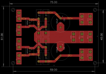
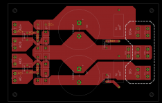
Hi everyone, hopefully I'm almost ready to order the pcbs to be manufactured. Here are the latest layouts. I've swapped out the spade terminals for signal, output & DC to molex ultra-fit. I've also included the remainder of the Thiele circuit on a separate PCB - I'm planning on bolting this directly onto the binding post terminals (hence the M8 pads), there are a couple of vias I can solder to if that doesn't work.
If you spot any problems, I'd be really grateful if you could let me know. Otherwise I'll go and order these.
Thanks,
Simon.
If you spot any problems, I'd be really grateful if you could let me know. Otherwise I'll go and order these.
Thanks,
Simon.
Attachments
What's going on with the stripey tracks on the right of the PSU PCB?
Yeah, I wasn't sure about that - it looks fine in Eagle so I guess it must have been an artefact of the conversion to png.
You have plenty of room to scoot C10 closer to the LM3886. I'd beef up the VCC pour even more. You're paying for the copper anyway. Might as well use it.
You're missing three components necessary for stability as the output voltage swings near the negative rail: Cc, Rf2, and Cf (see Test Circuit #2 on page 5 of the LM3886 data sheet).
I also suggest adding 47-100 kΩ from the input to GND on the "outside" of the input cap. This to prevent the input cap from collecting charge if the input is left floating.
Tom
Last edited:
You have plenty of room to scoot C10 closer to the LM3886. I'd beef up the VCC pour even more. You're paying for the copper anyway. Might as well use it.
You're missing three components necessary for stability as the output voltage swings near the negative rail: Cc, Rf2, and Cf (see Test Circuit #2 on page 5 of the LM3886 data sheet).
I also suggest adding 47-100 kΩ from the input to GND on the "outside" of the input cap. This to prevent the input cap from collecting charge if the input is left floating.
Tom
I'll squash up the right side of the board a bit more and increase the size of the vcc plane. I plan to solder Cc directly across the input pins on the underside of the pcb - that's why it's disappeared from the layout.
I have to admit that I'd completely confused myself about Rf2 and Cf and also mis-read the responses in this thread. Having read back through all the info I think I understand what they're there for I'll add them back in using the datasheet values.
When you say to add the resistor to the "outside" of the input cap does that mean between the signal input to the board (the molex connector) and the cap?
Thanks,
Simon.
- Status
- Not open for further replies.
- Home
- Amplifiers
- Chip Amps
- Newbie LM3886 Circuit