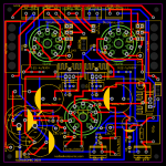
Ok. Like magic, I made it all fit in the wasted space between the 10uF caps using the parts on hand. I added a pot to adjust the delay length. The heaters must be 12VDC now but I think it should still work if referenced to B+ instead of ground.
Comments?
Comments?
Attachments

Sometimes suggestions like those here are good for making you learn how best to use space, a learning exercise either way 🙂
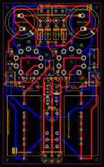
I would recommend using 45 instead of 90 degree bends on your traces wherever you can, it looks neater and is supposed to be less likely to cause defects in manufacturing. A minor tick that literally everyone saw fit to notify me of in PM when I first started out messing with PCBs. 🙄
Other than that it looks good.
Thanks, Ling.
News to me about the 90 vs 45. The board is black so you don't see the traces anyway but I'll keep it in mine. I might switch to arc instead of line, too.
How's this for efficient use of space? The little miracle PCB (because it does what it does in a 100mmx100mm square) can be triode, shunt screen pentode, or UL, and can use 6P43P or EL84 and the like 🙂 I originally used 1 600V cap, but I overlapped for 2 in series 🙂
I built the prototype boards up and they work well. The design was tested daily for a year in point to point by my 75 year old dad.
Attachments
Last edited:
I goofed! Wrong relay (it's NO, not NC) - Working on it.
EDIT: That's better.
EDIT: That's better.
Attachments
Last edited:
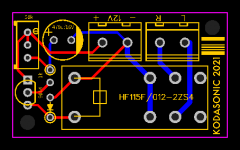
If you swap 240R and 1M, you get a silence machine. LMAO
Also, Today I learned 5W zeners need the leads left on to handle 5W. So if you build one of these, stand the zeners off of the board as far as you can 🙂
Also, Today I learned 5W zeners need the leads left on to handle 5W. So if you build one of these, stand the zeners off of the board as far as you can 🙂
For the OP cascode: I would use LR8 regulator(s) instead of Zeners. And since the current draw is constant, I would adjust the R drop so I don't need to dissipate too much.
LR8 and a pass device? if the zeners smoked, the LR8 would catch fire. I do have LR8 and TL431 though, and I have some DEP MOSFETs to use. I also considered omitting them and using a downstream regulator.
I think it's more of a matter of I didn't notice that the datasheet guaranteed the specs based on 3/8" leads. I had mine directly on the board severely derating them.
I think it's more of a matter of I didn't notice that the datasheet guaranteed the specs based on 3/8" leads. I had mine directly on the board severely derating them.
I kind of disagree with jean-paul's imbrication of not using 90° angles when also using 45° angles in the same circuit layout. At audio frequencies, it is kind of pedantic. But for digital, especially now that we're well past the 1970s, it makes a lot of sense.
As to board layout, I have to say I am totally old-fashioned, still liking a nice robust GND plane on one side or the other. Since I presume you layed this out using what, Eagle? or some such, its kind of a pain to do. Well, maybe it isn't any longer, since I've been out of the PCB layout business for better than a decade.
Consider watching make professional PCB at home with cnc prototyping machine WEGSTR - YouTube
Aren't those lovely one-off 'not-printed' circuit boards? Seriously way-cool. And the possibilities of a ground plane come 'for free'. WEGSTR … if you look at other videos, offers pretty compelling 2 layer design as well. No real need for plated-through connections, since for the level of production we're talking about, little wires soldered-on-both-sides-and-clipped-close do the job competently.
Also, seemingly falling out of vogue, is the idea of 0 Ω ('insulated wires') cross-over connections on PC Boards. I've found that all but the most obstinate designs can go from 2 layer to 1, with a handful of well placed 0 Ω wires. And they look kind of cool too, if you use 24 or 26 AWG, purple insulated solid conductor wire. Nice crisp runs, rounded corners, parallel orientation to the edges of the PCB.
Oh well.
I'm old.
I can't help myself.
⋅-⋅-⋅ Just saying, ⋅-⋅-⋅
⋅-=≡ GoatGuy ✓ ≡=-⋅
LR8 and a pass device? if the zeners smoked, the LR8 would catch fire.
No, what I'm saying is the LR8 doesn't need to dissipate much. Presumably the B+ coming in is reasonably filtered. You need to drop 280-250=30V. Why not adjust the 3.3k to drop 20V across it and 10V across the LR8? That's plenty to filter ripple. At say 10mA per cascode the LR8 would only dissipate 100mW per cascode. And you get real good regulation.
The Zeners dissipate a lot because they see the whole 250V and you need to draw some current to get any regulation. Essentially I'm saying in general shunt regulation wastes (and dissipates) a lot more power than series.
That makes more sense. For AF and even VF (NTSC), signals can go where you route them. Is it really that RF can't "turn corners"?
I lay out using EasyEDA (because it's easy). EasyEDA - Online PCB design & circuit simulator
I saw a tutorial about ground planes but since all of my circuits worked as point to point without one, and I can drag to resize the board easily without it, I thought it was more effort than it was worth. I would admittedly be rubbish at laying out radio.
I kind of disagree with jean-paul's imbrication of not using 90° angles when also using 45° angles in the same circuit layout. At audio frequencies, it is kind of pedantic.
It's not often that I see the words imbrication and pedantic in the same paragraph. The fringe benefits of erudite forum interlocutors 🙂
Also, seemingly falling out of vogue, is the idea of 0 Ω ('insulated wires') cross-over connections on PC Boards. I've found that all but the most obstinate designs can go from 2 layer to 1, with a handful of well placed 0 Ω wires. And they look kind of cool too, if you use 24 or 26 AWG, purple insulated solid conductor wire. Nice crisp runs, rounded corners, parallel orientation to the edges of the PCB.
⋅-⋅-⋅ Just saying, ⋅-⋅-⋅
⋅-=≡ GoatGuy ✓ ≡=-⋅
I call them "correction wires" lol Unless you use a 0 ohm resistor, it looks cheap to me. I use vias to simulate these now.
Last edited:
It's not often that I see the words imbrication and pedantic in the same paragraph. The fringe benefits of erudite forum interlocutors 🙂
A record for word definition lookups.
You may have noticed that having the current input- and output connectors changed in function i.e. input becomes output and vice versa, will lead to signal paths not crossing each other and way shorter and more elegant PCB tracks.
If the "new" inputs can be grouped and a 3 pin connector is used at the side of the board cabling to the PCB will be more elegant too.
If the "new" inputs can be grouped and a 3 pin connector is used at the side of the board cabling to the PCB will be more elegant too.
Attachments

Last edited:
Cut the track from "In L" and the one to "In R". Now connect the output cap tracks to that 3 pin connector and call it "L out" and "R out".
Change the former output connectors to be input connectors and adapt PCB tracks so they will be inputs.
In fact this is quite logical, no call it definitely most logical, as the input connector NOW is close to the output caps and muting relay and the output connectors are a few millimeters close to the input caps....
There will be no chance for coupling as input- and outputs tracks won't cross each other.
Last edited:
It's like the difference between a map and "Turn left at the post office" to me. Give me some time to attempt to decode it. Remember all the caps/relay/muting as an afterthought. The entire thing should be redrawn after a final design is found.
It is the art to use words to describe stuff. It is an art in German I can tell. In todays visual world it often leads to frustration but I won't stop doing it.
Just try to describe a certain form in detail to people and let them draw what you tell. You will be surprised. I call it "analog 3D thinking".
Just try to describe a certain form in detail to people and let them draw what you tell. You will be surprised. I call it "analog 3D thinking".
- Home
- Amplifiers
- Tubes / Valves
- NEW PCB: Active loaded triode High Z 9AJ voltage amp.