I routinely look at the input signal versus output this way. But you don't need anything but a good scope to do the SIM function. It must have channel inversion capability and add mode with variable vertical gain. You just add the two channels, one inverted and matched, and the differences are distortion.
I use a Tek 2235, which is considered a serviceman's scope, nothing fancy. I set it up on a 1 kHz sine wave, adjusting one channel down to get a flat line. Once it is set up, I apply other more challenging waveforms.
Ideally he waveform should be flat, but any deviations are the distortion products.
Hi all,
Hi Rode, good to hear from you. 🙂
I have used the SIM method ala osciloscope, 1 channel inverted and added... but the problem is that the dynamic range of the scope is too limmited.. setting the scope to 5mV/div.. I cannot use 2Vrms input as the scope clipped massilvely.. the adding/substracting bit must be done before going in the scope.. That's why the SIM method is more practical, isn't t?
As for FCD ... doesn't the fact that it is a very short transient type of distortion make it inherently difficult to see (and hear?) , either which method, SIM or not..?
I'll wait till I get my hand on copy of the article before I will begin to set my mind....
Best regards,
Thijs
rode said:
...A bootstrapped VAS normally has no effect on whether an amp will have that problem ["rail sticking"] or not. All of my designs are well behaved in that respect - they'd never make to the site if they were otherwise.
I normally drive the input with up to 10V RMS, then drop back to see the recovery time (should be virtually instantenous). .....Clipping behaviour is always thoroughly tested though, as it makes a big difference to how an amp sounds when (over)driven hard. ....
Some power opamps suffer from extreme rail-sticking, especially if they are driven to the limits. The sound is unbearable when it happens, as the harmonic content becomes extreme.
Regarding the queries of bootstrap linearity, it is not a problem over the normal operating range of an amp. At very low frequencies (where the bootstrap cap has significant reactance WRT the resistors), distortion does increase as the linearity of the bootstrap current source is reduced.
The -3dB frequency of the bootstrap circuit used is about 0.2Hz, so there is no significant degradation even at the lowest frequencies of interest.
Cheers, Rod
Well, I must quibble. A bootstrapped amp always seems to have a big startup thump, which I associate with charging the bootstrap cap. It's a minor negative, but bugs me.
And in MOSFET amps, the bootstrap voltage can exceed the Vgs limit at the extremes, if the amp supply voltages are high enough. That's because the bootstrap voltage is typically half the supply voltage, and the gate sees it through a resistor. Since there are usually zeners protecting the gate anyway, this is moot, but I don't like relying on them. I would prefer a diode clamp to the rail, as suggested by IR in the following app note:
http://www.irf.com/technical-info/an948/an-948p1.htm
Finally, a current source is supply voltage independent, while a bootstrap requires changing the resistors for a given supply voltage if you want to keep the current the same. I prefer to minimize adjustments like that. Of course, for the same reasons the CS has better power supply noise rejection.
Considering cost, it's nearly a push. A typical VAS transistor like an MJE340 costs about US $.29, in small quantities. Small caps are in the same range, maybe a tad cheaper. But caps dry out over 20 years, whereas transistors don't seem to age as rapidly. I say this because I work on a lot of vintage amps, and caps are some of the parts that fail most often. For that reason, I try to minimize their use.
I said these were quibbles. Logical but minor points. In the end, I am prejudiced and I know it. I prefer the precision and versatility of the current source loaded VAS implementation, even though I recognize both methods work well.
But on my cloud we do things my way. 🙂
tschrama said:Hi all,
...I have used the SIM method ala osciloscope, 1 channel inverted and added... but the problem is that the dynamic range of the scope is too limmited.. setting the scope to 5mV/div.. I cannot use 2Vrms input as the scope clipped massilvely.. the adding/substracting bit must be done before going in the scope.. That's why the SIM method is more practical, isn't t? ...
Well perhaps our scopes are different. On the TEK 2235, there is no problem having one channel on say 50mv/div and the second on 1V per division, inverted and varied to null with the other in "add" mode. That's what those controls are for, and they are indeed handy in this case.
The ratio between the gains is in fact set to the inverse of the gain of the amp. I'm surprised this does not work for you, but you certainly get the same result with the "SIM" method.
Probably not - different expectations perhaps. The difficulty with using a CRO (Cathode Ray Oscilloscope - common term in the UK and Oz, but would probably cause head scratching in the US 🙂 ) to measure the difference signal is that by the time you increase the sensitivity of the CRO enough to see the distortion, the front end amplifiers will overload.Well perhaps our scopes are different
For example, if you have a 20V RMS output signal, you will need the CRO set to perhaps 5mV/division before you see amp distortion, but by then, the front-end amp in the CRO is well and truly overloaded so the displayed waveform is meaningless. Even a 1V RMS input signal will cause the input amps to overload at 5mV/division. Assuming standard 8 divisions vertical, the amp will overload at about 16-32 divisions (double to quadruple the CRT full scale) or 80-160mV P-P. Even the higher figure is only about 56mV RMS.
This was one of the reasons I decided to look at the feedback signal rather than the output, but even then you will probably overload the oscilloscope's inputs. The SIM doesn't have that problem, since the differential amp nulls everything it can, and you can then add as much gain as you need to see the error signal clearly.
It's not a matter of different amplitudes, but a matter of the overload margin in the CRO. All that I have seen perform the summing function after the input amplifier, and that's where the problem lies.
Cheers, Rod
How about using fast diode limiter with resistor in series before diodes (some 200 Ohm - 500 Ohm) before the CRO input. I have done this because of the same problem (not audio measurement).
Pavel
Pavel
Nearly forgot this one 🙂
Well, if you were to build P3A, P68 or P101 (all use bootstrap), you would find that they all have zero thump at power on or off.
I agree that it's a negative, but if you are going to criticise a design, get your facts straight, and check the design before making derogatory comments about problems that don't exist.
All of the comments made show that the poster does not understand the design, has neither built or even simulated it, and is meerly quibbling for the sake of it.
I agree that a current source/sink is more technically elegant, but it lacks the 'elegant simplicity' of the bootstrap circuit. The proof is in the sound of the amp - my first production amp was sold to a recording studio, after they auditioned several different units, the second looks like it will do the same thing, and everyone who has heard it has been very impressed.
Although it is not immediately apparent until you really analyse the design, the boostrap circuit allowed the deletion of an additional 100V cap and a diode, over and above the two transistors (or one transistor and 2 diodes) required for an active current source.
Cheers, Rod
Well, I must quibble. A bootstrapped amp always seems to have a big startup thump, which I associate with charging the bootstrap cap. It's a minor negative, but bugs me.
Well, if you were to build P3A, P68 or P101 (all use bootstrap), you would find that they all have zero thump at power on or off.
I agree that it's a negative, but if you are going to criticise a design, get your facts straight, and check the design before making derogatory comments about problems that don't exist.
All of the comments made show that the poster does not understand the design, has neither built or even simulated it, and is meerly quibbling for the sake of it.
I agree that a current source/sink is more technically elegant, but it lacks the 'elegant simplicity' of the bootstrap circuit. The proof is in the sound of the amp - my first production amp was sold to a recording studio, after they auditioned several different units, the second looks like it will do the same thing, and everyone who has heard it has been very impressed.
Although it is not immediately apparent until you really analyse the design, the boostrap circuit allowed the deletion of an additional 100V cap and a diode, over and above the two transistors (or one transistor and 2 diodes) required for an active current source.
Cheers, Rod
Pavel, that rather defeats the purpose for this test. The idea is to make sure that the input and feedback points are not loaded to any appreciable degree, and the summed signal has to be as clean as the amp can make it.How about using fast diode limiter with resistor in series before diodes (some 200 Ohm - 500 Ohm) before the CRO input. I have done this because of the same problem (not audio measurement).
Only then can you see the distortion components that the amp contributes, as a difference between the input and feedback signals.
Cheers, Rod
Rod,
I did not read the posts patiently. You are right. Maybe the fast buffer before the limiter might help.
Pavel
I did not read the posts patiently. You are right. Maybe the fast buffer before the limiter might help.
Pavel
Millwood, it is already difficult enough for me to present my views, which are intended to improve reproduction for everyone, without you - *yet again* - pro-actively and provocatively following my posts in way that appears to non-technically challenge in a personal way !
____________________________________________________
Hi Rod,
I sincerely congratulate you on your SIM circuitry and suggested investigations, which you have freely shared with everyone.
To my knowledge you are still the only person trying to open peoples' eyes to this method of investigation, which can only be helpful. Your effort and the links are not new to me.
Regarding your last - sure we all like a little 'magic', but we do need to watch that the 'demons' don't creep in. As an aside I would add that we have all perceived the 'shifting images' and momentary sound stage 'phantoms' that arise within audio, yet even these electronically generated manifestations have entirely logical causes.
SIM - Either it is used to phase/amplitude alter the input signal in order to observe steady sinewave cycle distortion, or, it monitors already altered differential stage potentials.
As far as I am concerned, any waveform difference at the output/loudspeaker terminal wrt the source/input socket is distortion.
Connecting to the differential stage 'input' and 'NFB' nodes cannot indicate the same error waveforms that Slowhands can with his set-up.
Hi Slowhands,
If the bootstrap capacitor has a 2 to 3 secong time constant with its supply resistor, then there is no thump. However an unloaded bass cone might be seen taking an initial silent and shallow 'breath' prior to system usage.
Cheers ............ Graham.
Re: Nearly forgot this one 🙂
Unfortunately, I should not be held responsible for others' inabilit to comprehend and communicate. Sorry for that, Graham.
rode said:Well, if you were to build P3A, P68 or P101 (all use bootstrap), you would find that they all have zero thump at power on or off.
I can confirm that all the bootstrap circuits I have built (various versions of citation 12 and jlh1969) do not suffer from audible turn-on thump. My MOSFET version of jlh1969 did suffer from large turn-on thump but that has nothing to do with the bootstrap circuit used there.
Cheers, Rod
Graham Maynard said:Millwood, it is already difficult enough for me to present my views, which are intended to improve reproduction for everyone, without you - *yet again* - pro-actively and provocatively following my posts in way that appears to non-technically challenge in a personal way !
Cheers ............ Graham.
Unfortunately, I should not be held responsible for others' inabilit to comprehend and communicate. Sorry for that, Graham.
Can Not show here...
Can Not show here...
There is what that restrictions...
See beside me :
http://www.kievsat.com/phpBB/download.php?id=889
http://www.kievsat.com/phpBB/download.php?id=731
http://www.kievsat.com/phpBB/download.php?id=730
Can Not show here...
There is what that restrictions...
See beside me :
http://www.kievsat.com/phpBB/download.php?id=889
http://www.kievsat.com/phpBB/download.php?id=731
http://www.kievsat.com/phpBB/download.php?id=730
Re: Nearly forgot this one 🙂
A little testy there Rod, no criticism of you or your designs intended. Read my lips: "I said these were quibbles. Logical but minor points. In the end, I am prejudiced and I know it. I prefer the precision and versatility of the current source loaded VAS implementation, even though I recognize both methods work well. But on my cloud we do things my way. 🙂"
Lighten up dude! On your cloud, do it your way, but don't expect me to follow if I happen to prefer a different path.
Regarding implementing a current source in any of the referenced designs, it's much easier than you suggest. Simply replace one resistor with an appropriate transistor and tie its base to the existing reference (the LED anode in this case). Delete the bootstrap cap of course. For example, see the working example of a VAS current sink sharing a reference in this 1981 design by a certain gentleman:
http://www.passdiy.com/pdf/a40.pdf
Taking your P3A design, you replace R9 with say a BD139, tie its base to the LED anode, change R10 to say 150 ohms and you have a 7 ma current sink, no worries.
I don't see any need for the diode and cap you mentioned, simply because the CF pair is limited in voltage swing by its nature: the emitter of the driver Q6 is stuck to the collector of Q8, that limits the drive swing right there on upper and lower rails.
Are we going to hear a difference, in the same circuit using a bootstrap current source or an active current source? Probably not. I never suggested that. I proposed an alternative idea for designers to put in their bag of tricks, and use if they felt appropriate.
Which is what this forum is about.
rode said:
Well, if you were to build P3A, P68 or P101 (all use bootstrap), you would find that they all have zero thump at power on or off.
I agree that it's a negative, but if you are going to criticise a design, get your facts straight, and check the design before making derogatory comments about problems that don't exist.
All of the comments made show that the poster does not understand the design, has neither built or even simulated it, and is meerly quibbling for the sake of it.
I agree that a current source/sink is more technically elegant, but it lacks the 'elegant simplicity' of the bootstrap circuit. The proof is in the sound of the amp - my first production amp was sold to a recording studio, after they auditioned several different units, the second looks like it will do the same thing, and everyone who has heard it has been very impressed.
Although it is not immediately apparent until you really analyse the design, the boostrap circuit allowed the deletion of an additional 100V cap and a diode, over and above the two transistors (or one transistor and 2 diodes) required for an active current source.
Cheers, Rod
A little testy there Rod, no criticism of you or your designs intended. Read my lips: "I said these were quibbles. Logical but minor points. In the end, I am prejudiced and I know it. I prefer the precision and versatility of the current source loaded VAS implementation, even though I recognize both methods work well. But on my cloud we do things my way. 🙂"
Lighten up dude! On your cloud, do it your way, but don't expect me to follow if I happen to prefer a different path.
Regarding implementing a current source in any of the referenced designs, it's much easier than you suggest. Simply replace one resistor with an appropriate transistor and tie its base to the existing reference (the LED anode in this case). Delete the bootstrap cap of course. For example, see the working example of a VAS current sink sharing a reference in this 1981 design by a certain gentleman:
http://www.passdiy.com/pdf/a40.pdf
Taking your P3A design, you replace R9 with say a BD139, tie its base to the LED anode, change R10 to say 150 ohms and you have a 7 ma current sink, no worries.
I don't see any need for the diode and cap you mentioned, simply because the CF pair is limited in voltage swing by its nature: the emitter of the driver Q6 is stuck to the collector of Q8, that limits the drive swing right there on upper and lower rails.
Are we going to hear a difference, in the same circuit using a bootstrap current source or an active current source? Probably not. I never suggested that. I proposed an alternative idea for designers to put in their bag of tricks, and use if they felt appropriate.
Which is what this forum is about.
Indeed - although that was not really my intention. Consider me 'lightened up' 😀A little testy there Rod
I do know how to design a current source, but I'm always a little wary of using the same reference for the LTP and Class-A driver sources. There is a real possibility of cross-modulation because of the varying current into the (relatively) high current base circuit of the Class-A driver's current source. The LTP load is constant except under severe overdrive conditions.
The base current will vary, since the transistor has a wildly varying collector voltage, and unless the transistor used has the same Hfe at all voltages (very rare), the base current will change as needed to maintain the constant collector current.
There is also the loss of drive signal - negative drive in my case, but positive in some other designs. The bootstrap circuit can drive to well below (above) the rail voltage, so there is no drive swing limitation. Unfortunately this only affects one side of the amp 🙁
Any potential overvoltage is limited by the zener at the gate, however I have checked this, and the amp will clip before the zeners have to do anything. This limits the swing, and no greater voltage is available - one does not have to rely on the zeners to limit gate voltage except under output stage overload conditions.
The extra cap and resistor would normally be used in the negative supply rail. This is done in the positive rail, so that supply ripple is not applied directly to the drive circuit, and it also keeps the drive voltage at the maximum possible DC. The alternative is to use an auxiliary supply - this makes a big difference to very high power amps, but only adds complexity.
Because of the bootstrap, the amp effectively has an aux supply on the negative rail. Contrast this with a current source/sink, where one loses at least a couple of volts peak swing. In real terms it makes little difference of course, but as I mentioned before, I like the elegant simplicity of the circuit, and since it is anything but broken, there is no need to fix it 🙂
Audible differences? Probably not.
There is the potential for a current source to cause 'rail sticking' under severe transient overload - it has a relatively unlimited base current supply, so can fully saturate if driven hard enough, where the Class-A driver (VAS) has very limited base current resources - it can saturate, but can never go into 'super saturation' because there's just not enough base current available.
Again, audible? Probably not under proper conditions (minimal or no clipping).
I hope this explains my reasoning a bit better 😎
Cheers, Rod
Mo Powah
There are frequent posts here requesting more power from an amp. What would it take to increase power output from the P101? There are a few minor mods that can push it up a little, but this little design is pretty near the max. Here's the original:
http://sound.westhost.com/project101.htm
Increasing Output Voltage Swing
Lateral MOSFETs are somewhat limited in voltage ratings to 200v and below. The devices used in the P101 (Renesas 2SJ162/2SK1058) are rated 160v max, and Rod recommends operating them at a supply voltage of no more than +-70v, and lower for low impedance loads.
http://www.renesas.com/avs/resource/japan/eng/pdf/transistor/e2081182_2sj160.pdf
http://www.renesas.com/avs/resource/japan/eng/pdf/transistor/e2081244_2sk1056.pdf
If we had a very well-regulated supply, we might bump that to +-75v, but that would really be at the hairy edge, considering tolerances and noise -- the cruel real world.
Another approach is to run the front end and drivers from higher voltage, to compensate for the Vgs drops and driver losses. However, there are problems with this approach. As Rod has pointed out: "...using an auxiliary supply will make only a small difference ...The specified MOSFETs have a rated Vds (saturated voltage, Drain to Source) of 12V at full current, and that is simply subtracted from the DC value of the supply voltage."
Increasing current output by adding output devices
That's 12v worst case for a single device, but not for multiple devices in parallel supplying the same total current (say 7A). In the case of the P101, with two P channel devices running 3.5A, the drop is 6V max, 4v typical. If we add a third device in parallel, the numbers drop further to 4v max, 3v typical (comparable to a bipolar output stage.)
Similarly, Vgs needed for a given total Ids falls as per device current demand is reduced. So for say 3 devices in parallel, we only need a Vgs of 4v to for 7A total current.
Note: If you intend to run low impedance loads or bridge this amp with the high supply voltages, which Rod advises against, you must add output devices in parallel! Let's face it, Holton already does this on his similar amp, using quad outputs. See:
http://www.aussieamplifiers.com/sym-sch.htm
A modest increase in power
The upshot of all this is we can push this design a little but it's close to it's maximum output already, due to the output device voltage limitations and on resistance.
Here is one scenario: we could run the front end/driver at say 10v above the output devices, which would be conservative but still allow for driver losses and full Vgs for maximum current from the outputs. (You must upgrade the BC transistors to higher voltage parts, as well as the caps, diodes as appropriate). We still have the voltage drops through the output devices, which we can reduce a little with a 3rd device in parallel.
If we make those changes, I'd estimate only a 20% increase in power, from the present 180W to perhaps 220W. However, the reliability would be higher because the per device dissipation is lower. [Again, if you use high supply voltages and drive low impedance loads or bridge this amp, you must add output devices in parallel!]
Clearly, for significantly more power we need to go to higher voltage output devices, such as the Renesas 2SJ352/2SK2221. You could safely use +-90v rails with these, and expect something like 30% higher power, perhaps 240W. I'd definitely use more output devices per bank.
http://www.renesas.com/avs/resource/japan/eng/pdf/transistor/e2081193_2sj351.pdf
http://www.renesas.com/avs/resource/japan/eng/pdf/transistor/e2081352_2sk2220.pdf
Whew! That would be a lot of work for a modest increase in power. It does seem that the original design has hit the sweet spot for using these particular devices.
If you still want Mo Powah...
Multiple vertical MOSFETs with higher voltage ratings would be needed for truly significant power increases, and they would require significant temperature compensation not needed for the lateral MOSFETs. This is not really feasible to showhorn in to the P101, because you would need to add a Vbe or Vgs multiplier for that function.
I just bought some 500v Ixys complementary MOSFETs for fun and games.
http://www.ixys.com/94535.pdf
http://www.ixys.com/91536.pdf
The problem with these is the capacitance and on resistance is much higher than that of the lower voltage parts. Perhaps Holton's N-channel amp is a better option, because the N-channel devices are so much better than P-channel. To be continued....
True. If this is a serious problem, add an R/C filter to the base drive. I was being cheap.rode said:
...I'm always a little wary of using the same reference for the LTP and Class-A driver sources. There is a real possibility of cross-modulation because of the varying current into the (relatively) high current base circuit of the Class-A driver's current source.....
True again. The old RCA data books had little bootstraps to drive the other rail too, check out the 1966 edition for examples.rode said:
There is also the loss of drive signal - negative drive in my case, but positive in some other designs. The bootstrap circuit can drive to well below (above) the rail voltage, so there is no drive swing limitation. Unfortunately this only affects one side of the amp 🙁
Both the VAS and CS can stick. I put Baker clamps on both. It ends any possibiliy of sticking for either. When a device is saturated, the signal path is open, no signals can pass and the negative feedback loop is confused too. Best to minimize the duration.rode said:
.....
There is the potential for a current source to cause 'rail sticking' under severe transient overload - it has a relatively unlimited base current supply, so can fully saturate if driven hard enough, where the Class-A driver (VAS) has very limited base current resources - it can saturate, but can never go into 'super saturation' because there's just not enough base current available.
Again, audible? Probably not under proper conditions (minimal or no clipping).
Thx Rod/Repellant behavio(u)r
Board,
Regarding Rod E, I also cannot understand why others are so willing to take pot shots at his designs. Having built several of his amps, I can personally vouch for their elegant simplicity and outstanding performance. In fact, I'd be quite willing to provide a couple P3a monoblocks to compete against anything Graham has designed and built for under 500 pounds cost.
Thousands (and probably tens of thousands) of DIY'ers have benefitted from Rod's pages and projects resulting in a grateful and loyal following. I am not sure the same can be said for GM.
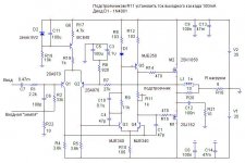
However, I do understand Graham is the creator of a nice insect repellant circuit.
http://geocities.yahoo.com.br/transistor548/repelente.htm
Graham's Insect Repellant Circuit
Being of Irish descent, I have an inherent and deep distaste for those who exaggerate their own self-importance. Thankfully Rod does not suffer from that affliction.
My opinions,
M
Board,
Regarding Rod E, I also cannot understand why others are so willing to take pot shots at his designs. Having built several of his amps, I can personally vouch for their elegant simplicity and outstanding performance. In fact, I'd be quite willing to provide a couple P3a monoblocks to compete against anything Graham has designed and built for under 500 pounds cost.
Thousands (and probably tens of thousands) of DIY'ers have benefitted from Rod's pages and projects resulting in a grateful and loyal following. I am not sure the same can be said for GM.
However, I do understand Graham is the creator of a nice insect repellant circuit.
http://geocities.yahoo.com.br/transistor548/repelente.htm
Graham's Insect Repellant Circuit
Being of Irish descent, I have an inherent and deep distaste for those who exaggerate their own self-importance. Thankfully Rod does not suffer from that affliction.
My opinions,
M
- Status
- Not open for further replies.
- Home
- Amplifiers
- Solid State
- New mosfet amp from ESP