Well I don't like doing listening reports since they can easily get flamed as being subjective, etc. However I think it is safe to say that the combination of the HPA-1 and the new Hifiman HE400se planar headphones is clearly the best combination that I have ever owned.
I suspect the HPA-1 is the best component in my system right now. I highly recommend it to fellow do-it-yourself fans. As for more involved listening reports perhaps I will leave that to the professional reviewers. I suspect that you will enjoy your project.
I suspect the HPA-1 is the best component in my system right now. I highly recommend it to fellow do-it-yourself fans. As for more involved listening reports perhaps I will leave that to the professional reviewers. I suspect that you will enjoy your project.
When I first powered it up I adjusted the offset, then bias and then repeated. I have not adjusted it since the first day.
I have not seen any bias stability issues. My heatsink does not get very hot. I am using one large heatsink (not individual heatsinks.)
Regarding offset a week later I turned it on without the servo to check and it went from -4 mV to 2mV then back down to -4 mV while warming up. With the servo enabled it is very low. One channel is 0.3 mV and the other is almost 0.0 mV. (I guess it depends on the op-amp variation.) If I remember I could disable the servo at the end of a long listening session and see what the offset is.
Last edited:
Thanks for the info. I was concerned about bias current stability, not so much DC offset. Putting the bias spreader on the heatsink would almost certainly overcompensate the output stage and make bias stability worse.
The output transistors for my board will mount to the chassis floor, like my other amps. I plan to bond the input pairs and the current mirror transistors together. I have no idea how much that really helps in practice, given the thermal resistance of the packages, but I like to imagine it makes me look like I know what I'm doing.
The output transistors for my board will mount to the chassis floor, like my other amps. I plan to bond the input pairs and the current mirror transistors together. I have no idea how much that really helps in practice, given the thermal resistance of the packages, but I like to imagine it makes me look like I know what I'm doing.
I meant to write "heat-shrink" the two input JFET together. I expect that will be sufficient inside an enclosure.
I will also use the aluminum chassis floor for heatsinking the outputs in the final assembly. I am still considering the pros and cons of various chassis for the final assembly.
I will also use the aluminum chassis floor for heatsinking the outputs in the final assembly. I am still considering the pros and cons of various chassis for the final assembly.
Is a 2SJ74 truly symmetrical, i.e., works exactly the same with the drain and source swapped?
Thanks.
Thanks.
It is supposed to like most j-fets but I would not build it as such.
Best answer I could find....
Actually, in general your statement is as wrong as it is right. Alot
of small signal FETS are equivalent when switching the drain and source.
Alot of special purpose or power FETS have structures that certainly would
disable or distroy the component if the 'drain' and 'source' were
interchanged. (Sometimes, it isn't the internal FET itself but it
is the protection circuitry that keeps inverse use from working.)
Not all fets work the same in 'inverse' mode, but again, most likely
such fets that do work are likely to be small signal
From a forum.
...but if you really want to get into it
https://global.oup.com/us/companion...on.websites/9780199339136/pdf/bonustopics.pdf 🙂
Jam
Last edited:
Thanks. The reason I asked is that the 2SJ74s are upside-down on Jeff Young's schematics. It's not obvious because his symbols don't have pin numbers, and the JFET symbol itself is symmetrical. The advantage of wiring them backwards is that the layout is cleaner when you place the input pair face-to-face.
From my reading, you can't be sure the device is symmetrical unless it says so on the data sheet, or you cut it apart and look at the physical structure. The difference is more likely to matter at RF frequencies. Out of an abundance of caution, or maybe just superstition, I've changed my schematic so the JFETs are oriented correctly.
From my reading, you can't be sure the device is symmetrical unless it says so on the data sheet, or you cut it apart and look at the physical structure. The difference is more likely to matter at RF frequencies. Out of an abundance of caution, or maybe just superstition, I've changed my schematic so the JFETs are oriented correctly.
Even if the device works with the source and drain switched I have been told that noise and gate leakage might increase.
In the HPA-1 (my personal unit), I attached the flat surfaces of the j-fets togther with some heatshrink (some thermal grease between surfaces wont hurt) just for better thermal trackibg but this might be acedemic for the most part in the real world (inside an enclosure).
Jam
In the HPA-1 (my personal unit), I attached the flat surfaces of the j-fets togther with some heatshrink (some thermal grease between surfaces wont hurt) just for better thermal trackibg but this might be acedemic for the most part in the real world (inside an enclosure).
Jam
Yes, I imagine in some devices they may tweak the chip geometry to optimize performance. The channel width varies as a function of gate-to-channel voltage, as does the capacitance, from one end of the channel to the other. I don't know much about semiconductor fabrication, but it just seems like a good idea to use the pins as designated.
People are reporting great results, and I bet many or most are just following Jeff's schematic schematic with no ill effect.
I'm still revising the layout. It feels a little cramped and busy to me.
People are reporting great results, and I bet many or most are just following Jeff's schematic schematic with no ill effect.
I'm still revising the layout. It feels a little cramped and busy to me.
I don't know the answer but in the Linear Systems datasheet for the complement (2SK170/LSK170) the breakdown voltages appear to be symmetric. This might be a clue. If anyone know for sure please post a reference.

I don't know the answer but in the Linear Systems datasheet for the complement (2SK170/LSK170) the breakdown voltages appear to be symmetric. This might be a clue. If anyone know for sure please post a reference.
Good observation. I think the odds are in favor that the transistor can be used in either direction without any problems. I do wonder whether Jeff made a conscious decision to do it this way, or if he just didn't think about it. As I said, I prefer to hide out over here, but you might ask him in the official thread.

Cute. 🙂
I've been spending hours working on the board. I substantially improved the organization of the resistors around the offset trimpots, and also cleaned up the relay driver. I've been checking everything very carefully, adjusting track registration, removing orphan traces, and trying to make the layout as symmetrical and precise as I can.
I was looking at other people's boards in the main thread. It's impressive how many good implementations there are, and how each designer takes a different approach. I think my own board is looking quite good now, though many of the changes will have no effect on performance, and you might not even notice some of them.
I don't know if anyone is interested in this, but I spend a lot of time just looking at the layout and trying to understand the flow of the circuit. If the layout is good (to me), it feels clean and unstressed. In a lot of ways, this work is like editing a text document, reading it over and over and trying to express myself as clearly and concisely as possible.
Well, this is all for today. I feel like it's close to a release candidate. I need to adjust some of the parts designators, and I think the relay connectors need to move down a little bit. I'd like the relay circuit to be more symmetrical, but it's not a symmetrical circuit, so the heck with it. Overall, the board seems like it's logically laid out now, and not too contrived.
For what it's worth, I thought hard about putting some attribution on the board but in the end decided it's best for several reasons just to label it "A3'". I appreciate the good work of everyone who had anything to do with the design of this project.


For what it's worth, I thought hard about putting some attribution on the board but in the end decided it's best for several reasons just to label it "A3'". I appreciate the good work of everyone who had anything to do with the design of this project.
So, looking back, I've posted four versions of this board. To me, that's like eight or ten hours of painstaking work since the initial layout, and each change SO important that every revision MUST be published. From the perspective of the casual viewer, meh, looks pretty much the same. LOL, I will stop posting my drafts.
I know that feeling - hours and hours of scrupulous work, all but invisible to those who haven't had their head stuck in you circuit gubbins 😀.So, looking back, I've posted four versions of this board. To me, that's like eight or ten hours of painstaking work since the initial layout, and each change SO important that every revision MUST be published. From the perspective of the casual viewer, meh, looks pretty much the same. LOL, I will stop posting my drafts.
Looking good!
Henry,
I apperciate anyone thst can layout a symetrical complementary circuit, looks like you understand the concept.
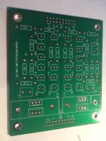
You have to learn to think up side down whlie being laterally inverted 😵 not an easy skill. This is not much a problem with two terminal non polar devices but when you introduce three terminal devices like transistors or fets, the hurt begins 😢. Some people have a difficult time or just plain can't do it. It took many hours for me to layout the attached board (complementary circuit- amp front end)
. It will get easier with practice.
It gets really hairy when you have to layout a balanced complementary symmetry design as in the second example.
Keep up the good work.
Jam
I apperciate anyone thst can layout a symetrical complementary circuit, looks like you understand the concept.
You have to learn to think up side down whlie being laterally inverted 😵 not an easy skill. This is not much a problem with two terminal non polar devices but when you introduce three terminal devices like transistors or fets, the hurt begins 😢. Some people have a difficult time or just plain can't do it. It took many hours for me to layout the attached board (complementary circuit- amp front end)
. It will get easier with practice.
It gets really hairy when you have to layout a balanced complementary symmetry design as in the second example.
Keep up the good work.
Jam
Attachments

Last edited:
- Home
- Amplifiers
- Headphone Systems
- New Headphone Amplifier Design