Yes, I know my inductance in the rails is high.
I became obvious when I had a look to the ringing and noticed
that the entire rail is ringing, when high di/dt occure.
Definitely a point for improvement. I am glad to get debugging support from somebody who has a deeper insider know how! 😎
Attached a principal scetch of the wiring.
...picture coming next....
Attachments
The high inductance of the rail seems not to be my issue.
I modified the circuit:
-Disconnected the upper drain from pos rail and connected it to the lower rail.
-Connected VS to the neg rail.
....just in order to examine the gate signals...
Now things seem to be even worse.
Originally the circuit was able to operate somehow, with some strange combinations of input voltage level, frequency and wave shape (triangle best).
Now it is hard to get any output signal. Sometimes a single pulse.
VDD, VCC and VB seem to be fine.
Maybe like the IRS20124S.....Look good on IRF web site, but unable to get it to work properly..I will never produce nothing with this IC...That's only good for cheap home theatre receiver! Shutdown always go on for no reason, lot of bizard thing happen with this, so I rapidely forget it! Anyways, you do a very good learning course with your project!
Fredos
www.d-amp.com
Fredos
www.d-amp.com
fredos said:Maybe like the IRS20124S.....Look good on IRF web site, but unable to get it to work properly..I will never produce nothing with this IC...That's only good for cheap home theatre receiver! Shutdown always go on for no reason, lot of bizard thing happen with this, so I rapidely forget it! Anyways, you do a very good learning course with your project!
Fredos
www.d-amp.com
+/-100VDC, it seems not your size at all. 😎
Hi Fredos,
well ...in general I am also not a fan of to many shut down mechanisms.
It does not make a big difference, if there is no music, because of burned components or because of protection. In both cases: No Music.
But I would not dare to generalize my issues with the IR chip.
And in the moment I still think, that with some R&D work I might get it running in a proper way. Otherwise I would already have switched to L6388.
The mostly identical but even worsen issues, when experimenting with the system on mostly power free conditions, is indicating to me that there is some hidden but probably really silly mistake on my side...
...search is going on...
Heureca
Making sense now...
In fact was struggling with multiple flaws....
The silly one first:
...because things have been really strange, I changed the simplest
input connection with VSS conected to COM....
==> no improvement, but I found that CSD was nicely ramping triangular between both tresholds...
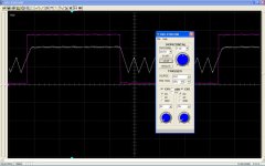
OK, in order to examine proper with my cheap scope, I changed the restart frequency. Means I speeded autorestart so that it is restarting within some hundred us. At the same time I applied low frequency input signals....
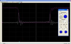
It became obvious that the upper MosFet was working without shut down.
White trace: Signal at CSD
Red Trace: IC output HO
Making sense now...
In fact was struggling with multiple flaws....
The silly one first:
...because things have been really strange, I changed the simplest
input connection with VSS conected to COM....
==> no improvement, but I found that CSD was nicely ramping triangular between both tresholds...
OK, in order to examine proper with my cheap scope, I changed the restart frequency. Means I speeded autorestart so that it is restarting within some hundred us. At the same time I applied low frequency input signals....
It became obvious that the upper MosFet was working without shut down.
White trace: Signal at CSD
Red Trace: IC output HO
Attachments
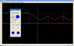
...hm, and what is LO doing?
With the resolution of the above pic: Nothing.
With slightly higher resolution: One single pulse of 1us length before every shut down.
So it is was definitely the shut down mechanism of the lower MosFet.
I rechecked the connections: fine
I measured the voltage between 8k2 and 1k2, which connected to OCSET: fine
I measured the voltage at OCSET: ...uhps!
Visually the connection was looking OK, but it had no electrical connection to the divider, but was floating close to zero. ...must have happened quite early, when I was playing around with various current limit levels...
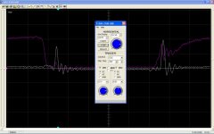
White trace: CSD
Red trace: LO
With the resolution of the above pic: Nothing.
With slightly higher resolution: One single pulse of 1us length before every shut down.
So it is was definitely the shut down mechanism of the lower MosFet.
I rechecked the connections: fine
I measured the voltage between 8k2 and 1k2, which connected to OCSET: fine
I measured the voltage at OCSET: ...uhps!
Visually the connection was looking OK, but it had no electrical connection to the divider, but was floating close to zero. ...must have happened quite early, when I was playing around with various current limit levels...
White trace: CSD
Red trace: LO
Attachments
...what else was troubling me?
Thing were still OK, after reconnecting the MOSFETs, but after rewiring it to a halfbridge and applying rail voltages... Things were not so bad, but also not really good.
-Additional 100uF directly across the HB-rails: slight improvement.
-100nF directly across the IC from VSS to COM: big improvement.
...at frequencies above 150kHz the driver supllies became weak.
==> OK, offering more supply current and skipped the 12 Ohms in series of the boot strap diode...
This altogether AND the fast gate drive circuit are making things quite promising (...just neglecting the fact that the 1N4937 is to slow for this application and is getting overheated, when running at 500kHz).
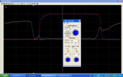
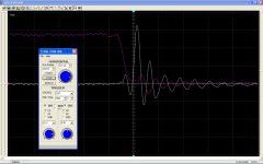
Have a look to the output of the halfbridge and gate drive of the lower MosFet, when running at 500kHz. Not so bad.
White trace: Ugs of lower MOSFET, 5V/Div.
Red trace: Uds of lower MOSFET, 20/Div.
Thing were still OK, after reconnecting the MOSFETs, but after rewiring it to a halfbridge and applying rail voltages... Things were not so bad, but also not really good.
-Additional 100uF directly across the HB-rails: slight improvement.
-100nF directly across the IC from VSS to COM: big improvement.
...at frequencies above 150kHz the driver supllies became weak.
==> OK, offering more supply current and skipped the 12 Ohms in series of the boot strap diode...
This altogether AND the fast gate drive circuit are making things quite promising (...just neglecting the fact that the 1N4937 is to slow for this application and is getting overheated, when running at 500kHz).
Have a look to the output of the halfbridge and gate drive of the lower MosFet, when running at 500kHz. Not so bad.
White trace: Ugs of lower MOSFET, 5V/Div.
Red trace: Uds of lower MOSFET, 20/Div.
Attachments
It's nice to see you're getting somewhere with it now. Nice work.
It'll be interesting to see how it looks once you've fine tuned the deadtime.
May I suggest since the output capabilities of this driver are so weak, and also since your mosfets may be of an older generation, that you buffer the output with some emitter followers?
Best Regards,
Chris
It'll be interesting to see how it looks once you've fine tuned the deadtime.
May I suggest since the output capabilities of this driver are so weak, and also since your mosfets may be of an older generation, that you buffer the output with some emitter followers?
Best Regards,
Chris
...yupp, optimzing the dead time, all suplies rails and may be the driver (hopefully not necessary to add much, but I will see...) will be my next steps.
Let's have a look to status quo. Some 2A/40ns current peaks in the wire between upper source and lower drain.
In fact this is not a proper measurement anymore, because taken with 50Ms. Means just two points for the peak. In fact the displayed magnitude is massively fluctuating, which also is indicating that my scope might miss something.... (But when I work with 100Ms, the triggering of that cheap scope is really annoying)
White trace: Current in the wire between both MosFets, 1A/grid
Red trace: Halfbridge output voltage, 20V/grid
Attachments
The peaks seem not to bee related to crossconduction.
There is something like 60ns real dead time, between finding the lower gate at zero and occurence of the peak.
... have to calculated/guess some Ixt area and parasitic capacitances if everything is matching together...
White trace: Current in the wire between both MosFets, 1A/Grid.
Red trace: Ugs of the lower MosFet: 5V/Grid.
Attachments
Here We Go
Attached the schematic of my final adjustment.
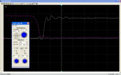
Real deadtime is... well let's say short.
If we start counting as soon as the Ugs is below the MosFet-treshhold of 5V, then we get something between 10ns...20ns.
If we start counting as soon as the Ugs is close to zero, then there is almost no dead time.
One unexpected nice feature. Behaviour does not change with temperature (at least not noticeable with my equipment). Always the same from 30C to 110C.
Attached the schematic of my final adjustment.
Real deadtime is... well let's say short.
If we start counting as soon as the Ugs is below the MosFet-treshhold of 5V, then we get something between 10ns...20ns.
If we start counting as soon as the Ugs is close to zero, then there is almost no dead time.
One unexpected nice feature. Behaviour does not change with temperature (at least not noticeable with my equipment). Always the same from 30C to 110C.
Attachments
I would not dare to speed up the sloping of turn ON, because of two reasons.
The non linear load of the switching MosFet is also influencing the driver output stage. With an gate resistor of 5 Ohms the IC is mostly triggered into some fault shut down. At 10 Ohms heavy reverse peak from Miller effect still can be seen at its output. At 15 Ohms it is still visible but OK.
And a second reason: dv/dt limit of the MosFets.
The max. dv/dt of the internal body diode for reverse recovery is specified with 5.5V/ns. This value is relevant when the amp might see a capacitive loudspeaker behaviour and the body diode might run the current, when the opposite MosFet is being turned ON.
Without load I am already at 6V/ns and ... well we can assume that sloping will be slower when the body diode is carrying current... But this has to be checked in detail as soon as the thing is grown to be an amp, not just a halfbridge.
White trace: Uds, 50V/Grid
Red trace: Ugs, 5V/Grid
Attachments
Markus, some of your solder connections look a little unwetted and blobby. That could be an indication of a cold joint and the reason why you had the bad connection. It's really tough to tell from a photo, but it looks like you could do well to leave the iron on for a few more seconds after the solder seems to melt. Also, when the surfaces to be joined are too oxidized, you may need supplemental flux either from a separate container or by applying excess solder until good wetting occurs. Of course, then you must remove (i.e., flick, wick, suck, etc.) the excess from the joint. Don't worry too much about time-related overheating with this method, because as long as new solder is being melted, phase change keeps the temperature steady.
Your photos and connections diagrams don't clearly detail how and if you separately route the output power connections from those nets common to the input circuits. You really want to avoid having high di/dts flow through shared signal lines. The power leads from the bench supplies should go only directly to the 2uF output capacitor leads with no stops in the signal/input section along the way. Connections to the small stuff should then come from these points. Actually, it's the minus supply routing that needs the most careful treatment. Ground for your board connections and measurements should ultimately come right from the plus lead of the 2uF capacitor stack by the low side MOSFET. The minus rail source for the board's layout should be the IC's COM pin.
Sorry for being pedantic, but have you verified the common mode integrity of your scope measurements? Check how much common mode noise your scope is picking up by momentarily moving the probe tip over to the supposed "ground" for the signal being measured. This is especially important for low level measurements (like current shunts). Common mode rejection can be improved by wrapping the probe cable several times through a large ferrite toroid (or clamp-on bead). Also, you may need to lose the probe ground wire/antenna and go to an on-board probe tip connector for the highest quality measurements. (By the way, how are you measuring current? If you are using some sort of current probe, does its delay differ from your voltage probes?)
You are wise to consider the reapplied dv/dt to a heavily recovering MOSFET body diode. I've seen otherwise outstandingly rated MOSFETs blow up at 10 percent of expected output power levels in a class-d application. IR devices are very conservatively specified in this regard, so, with those, you can go right up to (even a little past) the limit, IMO.
Rather than a simple gate driver diode, you might give the driver IC a break and discharge the MOSFET locally at its pins by using a Zetex style pnp BJT right on the MOSFET as an active pull down (its base-emitter is hooked up just like the diode with the "extra" collector pin soldered directly to the MOSFET source). This keeps the high discharge currents in a tight local loop.
Once you've got active discharge in place, it's easy to actively control peak dv/dt with very little impact on switching loss. For the simplest implementation, just add a series R-C in a very tight loop (minimal inductance is absolutely necessary to avoid making a multi-megahertz oscillator) right between the drain and gate pins of the MOSFET. The value of the "R" should be the same as the gate turn-on resistor and the value of the "C" should be about 2 or 3 times the MOSFET gate-drain capacitance measured at the level of the main supply voltage. The extra network is a true dv/dt limiter as it only steals enough drive to slow down dv/dt during fastest bit at the very end of the transistion.
Regards -- analogspiceman
YOU say my joints are looking blobby?! 😡
Hey!!! They ARE blobby. 😉 But I hope they are wetted, at least for my eyes they are looking alike.
My 80W soldering iron with fat tip is not what I prefer for SMD...
At least a smaller tip would be helpfull.
The not connected soldering was tricking me in another way:
It was looking fine, not even blobby. I looked from left, from right from upside... fine. I measured: Not fine. ...I looked again... hm, and again hm?!! From one special angle I could see it. The wire was not soldered at all, it was lifted about '0.nothing' mm from the joint... Never solder in a hurry !
Common mode integrity:
....is more or less OK...
I am using the same scope set up as during my 1kW boost converter, where I measured the small signals (around 1V) across a shunt resistor. This boost converter in critical conduction mode was definitely the most crazy idea (Eva: I agree... continuos mode with magnetic snubber might be a better solution for such power). The MosFets are turning OFF 20A within less than 30ns and slope Ugs with a snubbered dv/dt of 7V/ns from zero to 500V... ugly environment for small signals. But the measurements were quite low noise. I am running my probe wires through high perm torroids from VAC. Vitroperm material. In my experiments this gave much better results than ferrite. Especially with regard to lock up effects of the USB scope.... 🙄
My GND reference point for the scope was the source pin of the lower MosFet. If I connect scope GND and scope probe tip to this point, then I am getting something around 100mVp noise in the switching moment, which is acceptable for the Ugs measurement.
You are concerned about the remaining ringing of my Uds? 50% of this ringing is happening on the wire between upper source and lower drain. My postings show measurements at the lower drain. At the upper source is much less ringing, which is not surprising me. This wire is dealing with high di/dt. This di/dt will also run through the film caps and that wire inbetween, together probably making the other 50%...
For current measurement I am using a partially defect Tektronix P6021 (passive AC type, without delaying amp) .... Unfortunately I do not have any better test set up to check the timing relation between voltage and current than my half bridge.
Frankly speaking I do not have any reliable and fast test signal on hand at all... I shared your concerns before I saw the displayed signals. But the displayed timing of current peak and voltage sloping are matching unbelievably nice to my theoretically understanding. Don't you think so? I mean the sloping of the halfbridge and current peak are matching quite good, don't they? OK, that's not a a proper verification, but at least the displayed results do not cause timing doubts for me. I am more concerned about the magnitude...
GND wiring.
If you mean the small signals with "The minus rail source for the board's layout..." then I agree. Power is connected to the source of the lower MosFet, -also matching to your proposal.
But I am concerned what might happen if I run two half bridges.
There will happen an undesired HF loop, because of then two 100nF between VSS1/2 and COM1/2 (Loop: -4.8V, VSS1, 100nF,COM1, passing source1, some unavoidable GND connection, passing source2, COM2, 100nF, VSS2, -4.8V). Do you think I should add something like 100 Ohms between each VSS and the floating negative rail (-4.8V) ? And 100 Ohms between each VDD and positive floating rail (+4.8V)? These floating rails should supply later on both IR chips and some comparators...
Pull down PNPs... ...used this with good success for two paralleled bulky SPP17N80 in my boost converter, well I did not have these ZETEX devices and paralleled 5x BC560 (of course less fortunate in geometry)...
True dv/dt limiter: Good hint. Without that I would have tried it without the R. Just a cap between gate and source...
Which purpose does the resistor have? Damping unpleasant ringing effects?
Hey!!! They ARE blobby. 😉 But I hope they are wetted, at least for my eyes they are looking alike.
My 80W soldering iron with fat tip is not what I prefer for SMD...
At least a smaller tip would be helpfull.
The not connected soldering was tricking me in another way:
It was looking fine, not even blobby. I looked from left, from right from upside... fine. I measured: Not fine. ...I looked again... hm, and again hm?!! From one special angle I could see it. The wire was not soldered at all, it was lifted about '0.nothing' mm from the joint...
Never solder in a hurry !Common mode integrity:
....is more or less OK...
I am using the same scope set up as during my 1kW boost converter, where I measured the small signals (around 1V) across a shunt resistor. This boost converter in critical conduction mode was definitely the most crazy idea (Eva: I agree... continuos mode with magnetic snubber might be a better solution for such power). The MosFets are turning OFF 20A within less than 30ns and slope Ugs with a snubbered dv/dt of 7V/ns from zero to 500V... ugly environment for small signals. But the measurements were quite low noise. I am running my probe wires through high perm torroids from VAC. Vitroperm material. In my experiments this gave much better results than ferrite. Especially with regard to lock up effects of the USB scope.... 🙄
My GND reference point for the scope was the source pin of the lower MosFet. If I connect scope GND and scope probe tip to this point, then I am getting something around 100mVp noise in the switching moment, which is acceptable for the Ugs measurement.
You are concerned about the remaining ringing of my Uds? 50% of this ringing is happening on the wire between upper source and lower drain. My postings show measurements at the lower drain. At the upper source is much less ringing, which is not surprising me. This wire is dealing with high di/dt. This di/dt will also run through the film caps and that wire inbetween, together probably making the other 50%...
For current measurement I am using a partially defect
Tektronix P6021 (passive AC type, without delaying amp) .... Unfortunately I do not have any better test set up to check the timing relation between voltage and current than my half bridge.Frankly speaking I do not have any reliable and fast test signal on hand at all... I shared your concerns before I saw the displayed signals. But the displayed timing of current peak and voltage sloping are matching unbelievably nice to my theoretically understanding. Don't you think so? I mean the sloping of the halfbridge and current peak are matching quite good, don't they? OK, that's not a a proper verification, but at least the displayed results do not cause timing doubts for me. I am more concerned about the magnitude...
GND wiring.
If you mean the small signals with "The minus rail source for the board's layout..." then I agree. Power is connected to the source of the lower MosFet, -also matching to your proposal.
But I am concerned what might happen if I run two half bridges.
There will happen an undesired HF loop, because of then two 100nF between VSS1/2 and COM1/2 (Loop: -4.8V, VSS1, 100nF,COM1, passing source1, some unavoidable GND connection, passing source2, COM2, 100nF, VSS2, -4.8V). Do you think I should add something like 100 Ohms between each VSS and the floating negative rail (-4.8V) ? And 100 Ohms between each VDD and positive floating rail (+4.8V)? These floating rails should supply later on both IR chips and some comparators...
Pull down PNPs... ...used this with good success for two paralleled bulky SPP17N80 in my boost converter, well I did not have these ZETEX devices and paralleled 5x BC560 (of course less fortunate in geometry)...
True dv/dt limiter: Good hint. Without that I would have tried it without the R. Just a cap between gate and source...
Which purpose does the resistor have? Damping unpleasant ringing effects?
ChocoHolic said:
Which purpose does the resistor have? Damping unpleasant ringing effects?
Hi Spiceman!
This question was adressed to you...
I am really not sure about the pupose of RC instead of C.
...also my question about the HF loop....
P.S.
Yes, I would not bet on 100kh life time with 10k thermocycles ambient temp -40C...105C of my solder joints.... I am just playing around, for my living room.

Hello ChocoHolic
Just a question about your schematics...Why did you not derivated the VCC trought ground to limite the dissipation of your 3.3K 4W to a 1.5K 2W? Or better, trought the VSS pin to use only one power resistor? Just a hint to reduce component count and dissipation!
Have a nice day!
Fredos
www.d-amp.com
- Status
- Not open for further replies.
- Home
- Amplifiers
- Class D
- New half bridge driver IC with GND!! referenced input