....it might be a good idea to have the cap between VCC and COM roughly ten times larger than the cap between VB and VS.
Other wise the cap at VCC will be discharged at the first charging pulse for the cap at VB.
OK, now I added 1uF at VCC.
Hm, well at least I am getting some single pulses and VCC is looking stable enough (always above 11V). But still no proper operation.... annoying...
Anyway...., have to go to bed now.
Read U next
Markus
Hello Markus,
please try this:
switch a 10n...100n from Csd to Vss and put away the 8k2 pullup.
I´ll hope that current through the 3k3-4W is enough!?
Regards
Heinz!
please try this:
switch a 10n...100n from Csd to Vss and put away the 8k2 pullup.
I´ll hope that current through the 3k3-4W is enough!?
Regards
Heinz!
powerbecker said:please try this:
switch a 10n...100n from Csd to Vss and put away the 8k2 pull-up.
I´ll hope that current through the 3k3-4W is enough!?
Heinz hat recht. You'll likely get fault latching with an 8k2 pull-up. (Maybe that's what you wanted, but why not make use of the slow cycle auto reset capability?) But I'd go with something much bigger, say a 10u or so aluminum electrolytic.
Also, your input grounding setup is kind of weird, but it should work okay as long as the input test signal amplitude is a square wave and is big enough to get all the way down to Vss.
You might need to give the floating drive output a dc start up path so the start up lock out doesn't get stuck a power fault. Do this by adding a 10k resistor between the positive output supply and Vb. That's only half the path, so you will also need to add a 3k3 resistor between Vs and output ground.
Good luck -- analogspiceman
powerbecker said:If one reduce the Gate-Rs to 2E the current spikes seems
acceptable with short deadtime also the distortion is quite low.
A 2 ohm gate resistor is no problem for simulation but might require going beyond the limits of a realistic low inductance layout. These IR driver ICs are not rated to accept backwards currents through the outputs (only a very few driver ICs seem to be so rated). That means that the gate drive circuit resonance must be near critically damped so that the drive current can't flow through the IC substrate diodes on the resonance "back swing" when pinged by the switching edges.
For example, say the MOSFET equivalent gate capacitance is 5nF and the gate drive trace inductance is 80nH. Then the gate resistor should be no smaller than 2 x square root of L/C, which equals 8 ohms. Practically speaking a 1.5 x factor kills most ringing so a 6 ohm gate resistor should be okay. Even if you carefully worked the layout for minimum loop area and got down to 20nH, then the gate resistor should be at least 3 ohms.
I know what you're thinking, "but, the output impedance of the driver IC alone is 3 to 5 ohms!" That's actually a good point, but there's still IC power dissipation to consider. The f x C x V^2 losses appear in the gate resistor. With 400kHz 5nF and 15 volts (and 2 gates to drive), that's 900 mW of IC heating. Keeping the external gate resistors at least double the internal resistance reduces that to a much more comfortable 300 mW.
For these reasons I wouldn't expect to go with less than 10 ohms gate resistors, although lab experiments would always be the ultimate determination of best value.
Regards -- analogspiceman
Thanks Heinz & Aspice !
...well, yes I wanted to have latched shut down.
But with auto restart I was at least able to trigger reasonable signals with my poor kiddy scope. ... and there was a systematic relation between slight VCC sagging and shut down. By some reason the UVLO seems to act already at 11V and not 9.2V... or there is some unpleasant noise around, which my scope does not display...
I increased the VCC to roughly 14V, now it is running. Still sometimes hypochondric shut downs, but basically running.
Some wave forms soon.
Unfortunately they are looking as expected... means I am really wondering how to handle any timing in the range of some single ns !!!
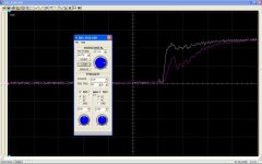
Now turning ON again and showing Ugs and Uds of the lower MosFet.
Halfbridge has no load connected. Due to MosFet capacitances we can expect that the half bridge will not slope during dead time.
Sloping takes place when the lower MosFet is turning conductive.
Turn ON delay is something like 50ns .... or so...
White Trace: Uds of lower MosFet, 20V/Grid
Red Trace: Ugs of lower MosFet, 5V/Grid
Attachments
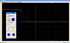
...the last measurement, before I have to go to bed:
Turning OFF and showing Ugs and Uds of the lower MosFet.
Turn OFF delay is something like ??!! .... or so... for sure above 100ns.
I am in the range of some cross conduction, even if there was not much heat generated, when running with 400kHz.
...have to examine this more detailed...
Also the 20MHz ringing of Uds is ugly and has to be cured.
White Trace: Uds of lower MosFet, 20V/Grid
Red Trace: Ugs of lower MosFet, 5V/Grid
Turning OFF and showing Ugs and Uds of the lower MosFet.
Turn OFF delay is something like ??!!
.... or so... for sure above 100ns.I am in the range of some cross conduction, even if there was not much heat generated, when running with 400kHz.
...have to examine this more detailed...
Also the 20MHz ringing of Uds is ugly and has to be cured.
White Trace: Uds of lower MosFet, 20V/Grid
Red Trace: Ugs of lower MosFet, 5V/Grid
Attachments

Welcome to reality
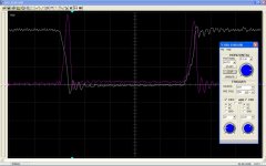
My fat MosFets are definitely the max limit, which this tiny driver can handle....
With the simple 22 Ohms gate drive, there are some nice crossconduction peaks around 7A for roughly 100ns...
This di/dt also caused the ringing, means the entire rail was ringing due to rail high inductance and only 2uF at the power stage. But rail ringing is no issue, because some larger fast caps at the power stage is smoothening this and without cross conduction this ringing is not triggered anyway.
When I parallel shottky diodes to the 22 Ohms in order to speed up the turn off with all available driver capability, then these crossconduction peaks go down to something like 1A/60ns. Well this seems to work, but is still ugly.
Unfortunately you cannot increase the 22Ohms for turn ON because this is delaying the turn ON to much and the overcurrent protection is shutting down, because sloping is not fully finished before the 200ns blanking is over ...
Hell !
I will have to play around with more non linear gate drive circuits, which do not charge the gate up to 13V, but to something like 8V-9V only...
Or I will have to look for some lower gate charge MosFets, but IRF540Z is slightly to weak... hm...
Or forgetting the IRS20954S and using a silly L6388?
Nice IC, but not suitable for high power MosFets.
I guess that's the reason why they state suitability for amps up to 500W. The limit will in many cases not be the voltage rating. Also not the thermal of the IC, but it's driving capability in combination with unpleasant short OC blanking. Unfortunately I do not see any option to enlarge the blanking time or disable the overcurrent protection of the low side FET. Is IR adressing to headphone amps with this IC ? 😀
Attached the ugly crossconduction with simple 22 Ohms gate drive.
(This condition can also sometimes trigger the shut down.)
Yes, of course I have already a better solution.... but this pic is more impressive ! 😉
White Trace: Uds, 20V/Grid
Red Trace: Current in the wire between upper and lower MosFet, 2A/Grid
Attachments
Why not add a simple discrete buffer after the chip, as resident gate drive expert Eva always suggests.
Just an unbiased push-pull emitter follower.
Just an unbiased push-pull emitter follower.
Hm...
IRF6665 seems to be a nice device. But it is to weak for my pupose, because I am going to run two paralleled 4 Ohm woofers from a +/-50V full bridge.
An additional discrete driver would probably help to speed up the Ugs sloping, but I am afraid of the group delay of such a buffer. It might cause similar issues as a slow dv/dt at the gate. ...up to now not tried, just a feeling from my stomach.
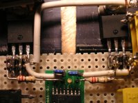
Also I made up my mind about the inductances in the gate drive.
But from my perception I would guess the inductive impedance of the attached wiring is much lower than the 22 Ohms gate resistor.
The white wires are the source connections between IC and MosFets and do not carry any load currents.
The gate resistors are placed mostly in line and the enclosed loop area appears not so bad for me. But I must admit: I am a HF-beginner.
IRF6665 seems to be a nice device. But it is to weak for my pupose, because I am going to run two paralleled 4 Ohm woofers from a +/-50V full bridge.
An additional discrete driver would probably help to speed up the Ugs sloping, but I am afraid of the group delay of such a buffer. It might cause similar issues as a slow dv/dt at the gate. ...up to now not tried, just a feeling from my stomach.
Also I made up my mind about the inductances in the gate drive.
But from my perception I would guess the inductive impedance of the attached wiring is much lower than the 22 Ohms gate resistor.
The white wires are the source connections between IC and MosFets and do not carry any load currents.
The gate resistors are placed mostly in line and the enclosed loop area appears not so bad for me. But I must admit: I am a HF-beginner.
Attachments
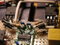
...also playing around with 18 Ohms and paralleled discharge diodes.
In order to reduce the inductances, I added an additonal straight wire between IC pin and source of the MosFet. The shottky diodes for discharging are directly connected to the IC and the MosFet. Also mostly straight geometry. Ugly looking, but more or less low inductive.
Nevertheless today, the shut down phenomen is quite strong, no matter if I use the older set up or the new one.
...not pleased in the moment.... May be there is another shut down mechanism, which is troubling me.
But it seems not to be related to my connection of the floating input, at least two other floating input connections and also input section bound to negative rail showed the same issues.
Attachments
Ivan hao!
...well, that's the relaxing point: I do not need it.
I probably can live pretty fine with a L6388 running at 100kHz.
But I found this IR chip quite promising. And I am just curious about my limits with high power devices. Especially after I noticed that here are some guys around, who seem to be able to handle timings in the range of single ns... !! So their designs seem to be about 50 times more precise than my beast. Making me envy
Ask those, "who seem to be able to handle timings in the range of single ns", to show THD/Power plot (not in the 1-10W region only). :lol:
analogspiceman,
nice German written! 🙂
Post 44:
I agree, it was only a simulation-try to get the lowest deadtime produced distorsion.
Markus,
I am afraid Your rocks (52N15D) are really to heavy for this cute driver 😉
If I were You I would start with much smaller ones and load.
After You see that ALL work satisfactorily with the small ones You can try bigger ones... may be with the suggested extra driver.
I can imagine that the additional delay is small in comparison to
the now used 18E Gate Resistor together with the big capacities from the 52N15D.
Also with this You´ll get the advantage to place them direct beside the fet with a smaller induction loop.
Regards
Heinz!
Hi Heinz,
...hm... you tell me my own words... "Try baby steps before playing with the big boys."
I will have to look for some small MosFets.
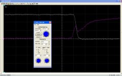
On the other hand I just measured the delay between ON signal of the lower gate driver output and the moment, when the output voltage of the halfbridge is touching the negative rail. In the setup of posting #54 I am measuring a delay of slightly less than 100ns. So I am not sure if I am still in trouble with the turn ON delay and 200ns shut down blanking.
Well, I can only measure this if the system does not shut down.
The poor triggering of my scope does not allow me to fetch the Also I repaired my differential probe and tried to measure the
moment of shut down with sufficient resolution.
Also I repaired my differential probe and tried to measure the VB.
Hm, probably OK. But my diff probe does not have a sufficient HF common mode rejection, so I cannot judge how much of the displayed peaks during sloping are reality or just a measurement error.....
...comes time, comes better understanding and a solution.
Unfortunately I have no chance to go on during the next days. May be Sunday, or may be the week end in ten days....
...hm... you tell me my own words... "Try baby steps before playing with the big boys."
I will have to look for some small MosFets.
On the other hand I just measured the delay between ON signal of the lower gate driver output and the moment, when the output voltage of the halfbridge is touching the negative rail. In the setup of posting #54 I am measuring a delay of slightly less than 100ns. So I am not sure if I am still in trouble with the turn ON delay and 200ns shut down blanking.
Well, I can only measure this if the system does not shut down.
The poor triggering of my scope does not allow me to fetch the Also I repaired my differential probe and tried to measure the
moment of shut down with sufficient resolution.
Also I repaired my differential probe and tried to measure the VB.
Hm, probably OK. But my diff probe does not have a sufficient HF common mode rejection, so I cannot judge how much of the displayed peaks during sloping are reality or just a measurement error.....
...comes time, comes better understanding and a solution.
Unfortunately I have no chance to go on during the next days. May be Sunday, or may be the week end in ten days....
ChocoHolic said:
I just measured the delay between ON signal of the lower gate driver output and the moment, when the output voltage of the halfbridge is touching the negative rail. In the setup of posting #54 I am measuring a delay of slightly less than 100ns. So I am not sure if I am still in trouble with the turn ON delay and 200ns shut down blanking.
It looks like you have short, minimal loop area connections directly between the G-S drive pins on the IC and the G-S pins of the MOSFET -- so far, so good. Unfortunately, the MOSFET power circuit is not completely visible in the photo. I can see one big wire between the top MOSFET's source and bottom MOSFET's drain, but not the rest of the loop (back around through the power supply capacitors). There may be enough inductance there to lead to forward biasing of the IC's substrate diodes during ringing peaks following switching. If that happens, bits of the IC can get flooded with carriers (which could possibly lead to the unexpected shutdowns you are experiencing). And on the subject of grounding, how are the ground connections made to each of the supplies and to the IC's input Zener's center point?
To make life easier for the IC you might try adding a 100nF (0.1uF) capacitor from Vss to Zener ground and add a fast diode (like the one to Vb) from Com (anode) to Vs (cathode). Place it right at the IC, pin-to-pin if you can.
For your information, I've run simulations of the various permutations of your test circuit (I modified one of the LTspice VDMOS models to reasonably match the important parameters of your MOSFETs). With the original corrected configuration (still the large gate resistors) the simulation shows HUGE cross conduction spikes, regardless of deadtime setting. But with the speedup diodes in place, you should be able to dial in as much as 60ns of deadtime (even with the IC's wimpy drive working into those large MOSFET gate capacitances).
Could you possibly post a photo that shows the rest of the test circuit wiring?
Regards -- analogspiceman
- Status
- Not open for further replies.
- Home
- Amplifiers
- Class D
- New half bridge driver IC with GND!! referenced input