I think Q11 is connected in wrong way on the schematic isn't it ?
I would agree, base and collector should be swapped.
photos ?
Reply to Slowhands re sizes
https://1drv.ms/i/s!AqqNLWgieBXciwKSDW2npujvKIPX if it doesnt work.
sizes internally 5 x 5 mm.
Reply to Slowhands re sizes
An externally hosted image should be here but it was not working when we last tested it.
Smashing outputs was theraputic.https://1drv.ms/i/s!AqqNLWgieBXciwKSDW2npujvKIPX if it doesnt work.
sizes internally 5 x 5 mm.
Last edited:
2nd attempt Probably fakes ?
An externally hosted image should be here but it was not working when we last tested it.
Last edited:
An externally hosted image should be here but it was not working when we last tested it.
Your photos are so funny. You took out your anger on those parts. I think this board has a lot of potential, and it's a bargain so it's worth analysis. Apparently there are many happy users of the board, so I'm thinking bad parts. The die you showed varied in area, and I think the smaller ones are fakes. The larger ones seem typical. Buy a real pair of IRFP240s and crack them open to compare. I have bought fakes from China, and they had tiny die inside power packages, to my loss.
Looking at the design, I don't see anything obvious which might cause failure. I would prefer an adjustment for bias voltage, but since this design does not have convenient source resistors to measure, you would have to use an ammeter on power leads. Easily done. But again, there is no adjustment. Add one.
The reason that matters is that MOSFETs can have large differences in threshold voltage from one to another. The spec is 2 to 4 volts, and most parts are about 3 volts, but you don't know. So the bias generator could be too low, or too high, and you can't control it. You need a trimmer to set this initially.
The next concern is the MOSFET as a bias generator. Does it really vary the bias properly? It is thermally coupled to the outputs, but it's running very low current. The thermal behavior of a power mosfet is not well specified at low currents. My inclination is to swap in a standard bipolar transistor Vbe multiplier, add a trimmer and see if that works better.
A subtle problem with mosfets is they like to oscillate at high frequencies due to stray coupling to the gate. It's random, depending on layout and lead dress. It can cause failure. I have seen 60-100 mHz oscillations in amps before, and they were difficult to quench. Often people give up and put big caps on the VAS output, which works but does not satisfy me. I like to put ferrite beads on the gate leads in all cases, since this goes a long way toward choking out the problem. I'll poke around on this board with a scope and see what's going on. Gotta buy some to investigate.
I mentioned there are no source resistors. MOSFETs can differ a lot in threshold voltage and on resistance. So there is no guarantee that 3 random parts in parallel will share evenly. Source resistors partly equalize the currents, but matching would be good too. I know they waste power, I know they cost money, but as it is you can have one MOSFET carrying all the current, until it blows, then the next carries all the current and blows, and finally number three blows. That's one scenario. They need to be matched and forced to share load.
So I'd add a trimmer and match the output devices. Verify the outputs are actual IRF240s by crushing one and comparing with a known good. Good luck.
wow a Lot to think about
Once again thanks and I have put my thinking cap on as to how these failed.
Whilst lots of people have had good results with this board and the L12 before I suspect that most are using normal CD as inputs rather than my wider band sacd/dvda outputs.
I state this as I noticed a slight problem with the Denon 3910 recently going,loud white output noise when misreading a DVDA disc.
This seems to cause a shut off on the Toshiba amp Im using as a temp.
As stated earlier I wasnt quite present at most of the 4 boards that blew but they were 2 @ reasonable level when I left the room...
One blew .! @ start up.1 @ normal level.Plus 1@ test level..
The System had DC blocking caps in all instaances..
The L15 boards were at med/high volume and I suspect 2 chips are still ok by measurement.No signs of damage from external view.
So it may be different or just one cause...
Still, I noticed those resister values you quoted are 68r..same on L20.?
This leaves me with possible oscillation of power supply ? as another common deminator in the failures.. Gave up my Scope almost 20 years ago and no current access to one.
I will take my lower level theruputic hammer to all the devices and record each check ,one by one.
Also as stated, I am awaiting L20 boards from Sep Sep but will be going away probably as early as this tuesday.
Its either of the two H s" ???? I would prefer Spain than the big building though.
Either way I intend to repair the L15 sans outouts at the moment.
Then possibly go bi active when All four boards are working.
Yep that is asking for trouble ?but life is short...LOL.
once again thanks for replies and I am looking for my suitcase next....
Some more thoughts
Looking at the design, I don't see anything obvious which might cause failure. I would prefer an adjustment for bias voltage, but since this design does not have convenient source resistors to measure, you would have to use an ammeter on power leads. Easily done. But again, there is no adjustment. Add one.
So I'd add a trimmer and match the output devices. Verify the outputs are actual IRF240s by crushing one and comparing with a known good. Good luck.
Had fun using my MSSH and ALLPF **on the outputs.
Photo with various chips.
two at the top and two (two pics)
two at bottom 3 pics)
The L12-2 devices at top left from Lazerlands defo look iffy.
https://postimg.org/image/4gica3heh/
Must admit I only measured DC offset at outputs to ensure low DC and it was very low and always seems to be on LJM kits.Except when they go wrong.
None of the working kits Ive used really got that hot, I will try meaurement of voltages at the relevant points before I connect up next time..
Meanwhile its Lazer replacement or adjustments to Denon.
**(Much Smaller Hammer and A Lot Less Physical Force)
PS
I noticed surfing the net that someone actually started listing fake Chinese parts
or is that REAL fakes ??? by die numbers etc..
That may be an interesting thread for this forum ? or not.
An externally hosted image should be here but it was not working when we last tested it.
The die you showed varied in area, and I think the smaller ones are fakes. The larger ones seem typical. Buy a real pair of IRFP240s and crack them open to compare. I have bought fakes from China, and they had tiny die inside power packages, to my loss.Looking at the design, I don't see anything obvious which might cause failure. I would prefer an adjustment for bias voltage, but since this design does not have convenient source resistors to measure, you would have to use an ammeter on power leads. Easily done. But again, there is no adjustment. Add one.
So I'd add a trimmer and match the output devices. Verify the outputs are actual IRF240s by crushing one and comparing with a known good. Good luck.
An externally hosted image should be here but it was not working when we last tested it.
Had fun using my MSSH and ALLPF **on the outputs.
Photo with various chips.
two at the top and two (two pics)
two at bottom 3 pics)
The L12-2 devices at top left from Lazerlands defo look iffy.
https://postimg.org/image/4gica3heh/
Must admit I only measured DC offset at outputs to ensure low DC and it was very low and always seems to be on LJM kits.Except when they go wrong.
None of the working kits Ive used really got that hot, I will try meaurement of voltages at the relevant points before I connect up next time..
Meanwhile its Lazer replacement or adjustments to Denon.
**(Much Smaller Hammer and A Lot Less Physical Force)
PS
An externally hosted image should be here but it was not working when we last tested it.
I noticed surfing the net that someone actually started listing fake Chinese parts
or is that REAL fakes ??? by die numbers etc..
That may be an interesting thread for this forum ? or not.
Last edited:
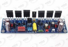
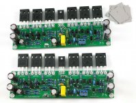
The designer, LJM, mentioned in an earlier post that there is a similar version of this L150W amp with complementary output MOSFETS that sounds better. It is called L150. I am posting pictures below of the L150W and the L150. (I am ignoring the similarly named digital amps L150D and L150SMD).
Neither the L150W nor the L150 has source resistors to balance currents in the MOSFETs. Neither has zeners to protect the MOSFET gates from excessive voltage. The L150W has about 9 small signal transistors, while the L150 has 16. The circuits must be quite different. We have an approximate schematic for the L150W, but none yet for the L150. I will try to get one.
Though flawed, these amps are cheap and small. They are a good starting point for mods.
Attachments
150w versions ????
We have an approximate schematic for the L150W, but none yet for the L150. I will try to get one.
Though flawed, these amps are cheap and small. They are a good starting point for mods.[/QUOTE]
Thanks again , It appears mine is a 150W/2 and it had differrent values to the initial 150W.As I stated. So there may be three versions... Mine had NO 100k and a lot more 10k and 2k2 resistors.
Ironically I am just removing one of the 150Mf caps from that boards...It is to replace a faulty one on the L20/ ver 9.2 which I have just reported faulty(yet again) on another thread .
http://www.diyaudio.com/forums/solid-state/296749-ljm-l20-v9-0-amplifier-3.html
It looks like the pos leg is broken possibly due to bending or pressure when packed.
Dave
The designer, LJM, mentioned in an earlier post that there is a similar version of this L150W amp with complementary output MOSFETS that sounds better. It is called L150. I am posting pictures below of the L150W and the L150. (I am ignoring the similarly named digital amps L150D and L150SMD).
Neither the L150W nor the L150 has source resistors to balance currents in the MOSFETs. Neither has zeners to protect the MOSFET gates from excessive voltage. The L150W has about 9 small signal transistors, while the L150 has 16. The circuits must be quite different. We have an approximate schematic for the L150W, but none yet for the L150. I will try to get one.
Though flawed, these amps are cheap and small. They are a good starting point for mods.
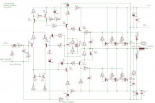
Some corrections, and a possible schematic of the L150W V2. First, the complementary output version is called L15. Second, there are zeners on the gates in the L150W.
I will be looking in detail at the L150W V2 as soon as I receive boards. I post below an approximate schematic, which is merely a transcription of what LJM posted earlier into Eagle schematic capture program. This has not been checked against an actual board so will have discrepancies. Best I have now. This appears very similar to Quasi's quasi, except for parts values.
Attachments
Some corrections, and a possible schematic of the L150W V2. First, the complementary output version is called L15. Second, there are zeners on the gates in the L150W.
I will be looking in detail at the L150W V2 as soon as I receive boards. I post below an approximate schematic, which is merely a transcription of what LJM posted earlier into Eagle schematic capture program. This has not been checked against an actual board so will have discrepancies. Best I have now. This appears very similar to Quasi's quasi, except for parts values.
This is a related topic about another LJM amp board, the L20se. I ordered a couple of PCB+parts kits that I will be building. I wanted to know the input Dc-blocking HP filter corner frequency so I traced the board and found that the input cap and preceding drain resistor did not exist on the board (but were in an L20v9 schematic that someone posted).
Can you verify that parts R1 and C1 are actually on the board you are looking at? I'm just curious about that...
missing R1
Can you verify that parts R1 and C1 are actually on the board you are looking at? I'm just curious about that...[/QUOTE]
I have the w150 ver 2 which failed as reported.It was missing the 100k resistor but had C1 .
I also have L20 v9.2 This has both and a lot more parts later
D
Can you verify that parts R1 and C1 are actually on the board you are looking at? I'm just curious about that...[/QUOTE]
I have the w150 ver 2 which failed as reported.It was missing the 100k resistor but had C1 .
I also have L20 v9.2 This has both and a lot more parts later
D
Hmmm, that's interesting because I thought the L20v9 and the L20se were the same thing, apart from 2x the output transistors in the v9 (and associated parts). Maybe that is too naive of me to think that.I also have L20 v9.2 This has both and a lot more parts later
D
In a pic of the 9.2 I can see that the board (on the input side of it) was widened compared to the L20se so that the input cap could be accommodated. The 100k resistor (R1?) is just a drain resistor for draining off DC charge on the input cap. You could add it.
A 1M0 or 2M2 could be added across the input socket along with a 47pF to act as a first stage RF filter............The 100k resistor (R1?) is just a drain resistor for draining off DC charge on the input cap. You could add it.
Both could be 805 smd for a small loop area.
That MOD would be impossible for me (now)
Hi Andrew again and thanks again.
Sadly my recent eye ops have been a disaster for close-up work even with assistance.I can now see the man in the moon better ?
I am now using the 20 version 9.2 and just finished setting up into a case.So plans to rebuild the spare 150w are cancelled and the almost new boards including many parts are for sale or near givaway.Along with a few L120s.
Only other comment re that 100k resistor or even 47ks in the older days (Plenty of them) in that location.Dave
I always noticed that changing that to a vishay bulk foil still effected the sonics.Just like the signal path resistors. Ears and brain are my current measuring devices .
A 1M0 or 2M2 could be added across the input socket along with a 47pF to act as a first stage RF filter.
Both could be 805 smd for a small loop area.
Components for input RF filtering are already present.
Any one have experience with the amp in this thread (L 150w) and LJM's L15 mosfet?
Curious because there are differences, but I'm am unsure which is better, cleaner, less distortion amp.
Additionally - do they put out the same power? Sellers on eBay vary in the output ratings.
Looking to run a stereo pair at +/-65vDC with 40-60kuF power supply and 600VA toroidal.
Curious because there are differences, but I'm am unsure which is better, cleaner, less distortion amp.
Additionally - do they put out the same power? Sellers on eBay vary in the output ratings.
Looking to run a stereo pair at +/-65vDC with 40-60kuF power supply and 600VA toroidal.
Hmmm, that's interesting because I thought the L20v9 and the L20se were the same thing, apart from 2x the output transistors in the v9 (and associated parts). Maybe that is too naive of me to think that.
In a pic of the 9.2 I can see that the board (on the input side of it) was widened compared to the L20se so that the input cap could be accommodated. The 100k resistor (R1?) is just a drain resistor for draining off DC charge on the input cap. You could add it.
You are not wrong. L20v9.2 and l20se are the same circuit.
It's just that l20v9.2 has eight transistors.
A 1M0 or 2M2 could be added across the input socket along with a 47pF to act as a first stage RF filter.
Both could be 805 smd for a small loop area.
You don't need to add these things.
It won't do any good. Enter LPF. The main purpose is to prevent high frequency interference.
As long as there is no interference. That's OK. Good.
Any one have experience with the amp in this thread (L 150w) and LJM's L15 mosfet?
Curious because there are differences, but I'm am unsure which is better, cleaner, less distortion amp.
Additionally - do they put out the same power? Sellers on eBay vary in the output ratings.
Looking to run a stereo pair at +/-65vDC with 40-60kuF power supply and 600VA toroidal.
Relatively speaking. L15 is better.
Use irfp240 9240.
Hello LJM....I am about to make another of your excellent amplifiers (L20 v9.2 shown in photo) and wish to buy a MOSFET design. I would like to buy either the L150W or the L15....so I was wondering WHY is the L15 better than the L150W please?...Very much obliged if you could take the time to help me here...Thanks.Relatively speaking. L15 is better.
Use irfp240 9240.
Attachments

Last edited:
- Home
- Amplifiers
- Solid State
- New Design L 150W FET Amplifier