Re: AD SRC
1:Looking good here to-> But you have short circuited R44,45 and R46.
2: No change is needed they got the same pin layout.
3: Good option like that🙂
pred said:Here there are a lot of changes:
1. There are two clocks and their corresponding clocks. For AD1896 you have to put it into the slave mode so there are additional chips.
2. For the 27MHz+ clock for the AD I predicted both CMOS clock or simple quartz since the quality is not critical
3. One can decide on the mode of operation using jumpers (slave or master)
What to look for:
1. As before look for errors and check that everuthing is correct.
2. Check is there a thing to change in order to be compatible wiht BB SRC chip, since it can work on 192k from 1 clock (some say it is wors sonicaly)
1:Looking good here to-> But you have short circuited R44,45 and R46.
2: No change is needed they got the same pin layout.
3: Good option like that🙂
Re: DAC
It´s also looking good here.
I don´t know if we should call it "your project"......
Kim
pred said:Dac schematics are posted for the first time.
Check them for errors. Make wishes for changes. I also have jumpers in order to change the mode of opperation. In this way you can use each in mono or two in stereo in paralell.
That is it. Hope you have energy to continue.
Since I am puting most of the energy into this project I think I have a right to name the dac. Although maybe done so many times in the past I have decided to name it after my daughter Sofija (yes there is a "j" in the name, it is not an error). Hope you do not mind.
It´s also looking good here.
I don´t know if we should call it "your project"......
Kim
rfbrw said:I would suggest you use the '163 synchronous counter. Not only does it have a uniform propagation delay across all 4 Q outputs it also clocks on the same edge as the '74. This means signals heading for the D input of the '74 can have a nice meal, wave to Darth Ulas and still be stable in time for the arrival of the next 24 meg rising edge.
Yet another diyAudio expert who doesn’t read data sheets or understand basic digital circuits. The only reason for the ‘74s following the ‘4040 is to “unripple” the output. Using a synchronous counter obviates their need altogether.
I don’t think your ‘163 suggestion will help Pred. He needs more than 4 stages. Since he doesn’t read datasheets, how do expect him to daisy chain two counters.
Ulas said:
Yet another diyAudio expert who doesn’t read data sheets or understand basic digital circuits. The only reason for the ‘74s following the ‘4040 is to “unripple” the output. Using a synchronous counter obviates their need altogether.
One might think the '74 superfluous and in a similar situation choose to leave them out but it isn't my design and I have seen enough commercial designs to know that registering a registered device is not uncommon. I also lack the conceit to insist I know best in all circumstances and my way is the only way.
I don’t think your ‘163 suggestion will help Pred. He needs more than 4 stages. Since he doesn’t read datasheets, how do expect him to daisy chain two counters.
No ****, sherlock. Of course, he needs more than a single '163 but, your contempt notwithstanding, I'm sure he'll figure it out.
Re: Board layout
Could you be more specific about this? I do not understand what is your wish. If you mean placement on the PCB, that will be done later, these are only schematics for the moment and do not relate to the PCB .
Pred
Cobra2 said:you could moove the small caps (C2,....C6) closer to the CS84xx pins, IMO.
Arne K
Could you be more specific about this? I do not understand what is your wish. If you mean placement on the PCB, that will be done later, these are only schematics for the moment and do not relate to the PCB .
Pred
rfbrw said:No ****, sherlock. Of course, he needs more than a single '163 but, your contempt notwithstanding, I'm sure he'll figure it out.
Thank you in having the faith in me 🙂. I understood from the start what Ulas wanted to say. I must admit that I have red the datasheet but not in detail. It is puzzling that when you calculate the worse case scenario for the propagation you get to the 22MHz operation of '4040. But still the manufacturer claims to have 80MHz operation! Maybe I am reading it in a wrong way, but I thought if he means 80MHz it will work in any case, and that was around 3 times more than I needed. I must admit that different clock edges was an error and will remedy it, ASAP. The problem is that farnell does not stock 74VHC163 over here so I have to look little bit closer what to do.
As for the last Ulas post: I do not deal with rude people, so no comments on your messages from me in the future.
Hi, yes I know I am late. Sorry if someone is waiting and is impatient. I have familly to feed so I was pressed to do some other stuff. If everuthing go as planned I will finish the PCB till new year.
I attach the ad src part of the schematics. I included some changes that you wished for. I "figured out" 😉 how to divide the clock. Some of the delay is also due to the fact that I could not find vhc161 or 163 near me. Finally I did. For those that are not familiar with parts they are both counters, one is with sinchronous reset other is not. For this application it does not matter.
Other big change is for the oscillator. Firs for the CMOS clocks I have added two resistors for enable. I think I saw some on the net that are enabled on low other on high en pin so I made possibility for both. Also, for the quartz part that is another option I have included a posibility to add serial quartz (3rd harmonic?) I have never used one in my life so I have copied the schematics from the AD datasheet. I hope that small resistor Rosc2 will not disturb oscillations on 30MHz via some parasitic capacitance effects...
Tell me if you want to have some more changes.
Attachments
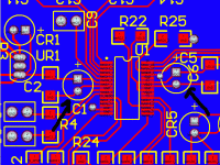
pcb question
I have started to work on a pcb. I did some of it but have a principal qustion on grounding. I have red recomendations of Guido on grounds and that he connect the ground of a chip right at the pin, then he has a connection to the capacitor (or two) but does not connect them to the ground (if they are leaded components).
I have included part of the layout. Blue is bottom ground plane and red is top copper. If you look at two decoupling capacitors (there is a rather ugly black arrow pointing at them 😎 ) in my opinion they are quite close to the chip it self. I can put the via to the ground plane near the chip pad and it will be closer 2.3mm then if I use capacitor lead for the grounding. Is these 2mm so important. I ask this since it is also helping my layout in a huge way. If I use separate connection then I would have to make the ground plane and then connect by hand every other component to it. A lot of work and rather prone to errors.
Do you hace any sugestions on this subject?
Attachments
Pred,
Before you waste more time on a PCB layout and before you waste any money getting PCBs made, you should read and understand the datasheet of every part used in your design. Pay careful attention to input requirements and output specifications.
Before you waste more time on a PCB layout and before you waste any money getting PCBs made, you should read and understand the datasheet of every part used in your design. Pay careful attention to input requirements and output specifications.
Ulas said:Pred,
Before you waste more time on a PCB layout and before you waste any money getting PCBs made, you should read and understand the datasheet of every part used in your design. Pay careful attention to input requirements and output specifications.
Thank you, I'll might just do that.
Pred
Hi Pred,
Aside from the basic digital logic errors that will keep your DAC from working at all, errors that are so obvious to me, like the ‘4040, I am amazed none of the diyAudio experts have spotted them, I was curious about your other design decisions. Why do you pump up the sample rate to 192K? According to the datasheet, the ‘1794 gets its best dynamic performance with a 44.1K sample rate. Every doubling of the sample rate doubles the THD+N.
Why convert the sample rate at all. Jitter reduction? HA. The basic function of an asynchronous sample rate converter is to measure the difference between the incoming and outgoing sample rates and interpolate the sample data accordingly. To measure a time differential, you need a precise time reference. That’s what the master clock is for. Any instability or jitter in the master clock will result in erroneous interpolation. Your master clock is an ordinary crystal or XO and its jitter will be permanently embedded in the signal. If you really need ASRC, you should put your money into the master clock.
If you really want to drastically reduce jitter, you don’t need snake oil XOs, PLLs, or ASRC. You already have the basics in your design. All you have to do is recognize it and remove of the superfluous crap.
Hi,
first I want to underline that I never proclaimed my self an expert. At least not for this project. I might be called one for some other areas of electronics, not jittering, ascrs and clock stuff. I am on the front line just because I accepted to be a workhorse and hope someone else would enjoy as well. I just thought (maybe I was wrong) that we are all friends here having fun. I never thought to earn money here, at least not with this project anyway. Looking how audio as a bussiness holds it is not for me. And that is where I stand. Nothing more nothing less. This is excursion from the project and I will not come to it again in future
I looked at the ADSRC part and appart one ground connection I do not see any problem with inputs and outputs. The only thing that is left for checking is inverting of LRCK (I used flipflops instead of inverter). That stayed from some previous discussions and I will have to see if this is necessary. If you see something I don't I would appriciate a bigger pointer.
The basic idea was to have a DAC that can accept frequencies up to 192kHz. The second was as modular as possible. For me what is interesting is that external (as well as internal) filters will mess less with the audio range if the signal is on higher sampling rate. THD that is doubling is still quite low. I did test myself some years ago on how much THD can I hear. I was "disapointed" that if I was honest with myself I could not hear bellow 1%. So if the thd is 0.0001 or 0.001 for me it is zero importance...
We had to use XO since it is available for everyone and does not promote anyone else. Deliberate decision is to use DIP package since you will have holes and can add external clock of your preference and quality. So you can start with XO and than build up, real DIY style. I did not wanted to use eather kwak, guidos or LC clock. That way I would decrease number of people interested in project. I do not dream it will be a huge success, but still more open will put more people into the game. The system is so open you can run ASRC on 44.1kHz and if you want I will add couple of holes on the pcb so you can directly bypass the ASRC alltougether.
That is it from me I will continue to work on the design and I would appriciate your help if you are prepared to share your knowledge here with us. If you think you have a better idea and know the way to ulitmate pleasure in digital music reproduction you can always, with a couple of clicks, start your own thread. Here, we do not promise anything.
Again, thank you for the help you have given us so far.
first I want to underline that I never proclaimed my self an expert. At least not for this project. I might be called one for some other areas of electronics, not jittering, ascrs and clock stuff. I am on the front line just because I accepted to be a workhorse and hope someone else would enjoy as well. I just thought (maybe I was wrong) that we are all friends here having fun. I never thought to earn money here, at least not with this project anyway. Looking how audio as a bussiness holds it is not for me. And that is where I stand. Nothing more nothing less. This is excursion from the project and I will not come to it again in future
Ulas said:Pay careful attention to input requirements and output specifications.
I looked at the ADSRC part and appart one ground connection I do not see any problem with inputs and outputs. The only thing that is left for checking is inverting of LRCK (I used flipflops instead of inverter). That stayed from some previous discussions and I will have to see if this is necessary. If you see something I don't I would appriciate a bigger pointer.
Ulas said:Why do you pump up the sample rate to 192K? According to the datasheet, the ‘1794 gets its best dynamic performance with a 44.1K sample rate. Every doubling of the sample rate doubles the THD+N.
The basic idea was to have a DAC that can accept frequencies up to 192kHz. The second was as modular as possible. For me what is interesting is that external (as well as internal) filters will mess less with the audio range if the signal is on higher sampling rate. THD that is doubling is still quite low. I did test myself some years ago on how much THD can I hear. I was "disapointed" that if I was honest with myself I could not hear bellow 1%. So if the thd is 0.0001 or 0.001 for me it is zero importance...
Your master clock is an ordinary crystal or XO and its jitter will be permanently embedded in the signal. If you really need ASRC, you should put your money into the master clock.
If you really want to drastically reduce jitter, you don’t need snake oil XOs, PLLs, or ASRC. You already have the basics in your design. All you have to do is recognize it and remove of the superfluous crap.
We had to use XO since it is available for everyone and does not promote anyone else. Deliberate decision is to use DIP package since you will have holes and can add external clock of your preference and quality. So you can start with XO and than build up, real DIY style. I did not wanted to use eather kwak, guidos or LC clock. That way I would decrease number of people interested in project. I do not dream it will be a huge success, but still more open will put more people into the game. The system is so open you can run ASRC on 44.1kHz and if you want I will add couple of holes on the pcb so you can directly bypass the ASRC alltougether.
That is it from me I will continue to work on the design and I would appriciate your help if you are prepared to share your knowledge here with us. If you think you have a better idea and know the way to ulitmate pleasure in digital music reproduction you can always, with a couple of clicks, start your own thread. Here, we do not promise anything.
Again, thank you for the help you have given us so far.
pred said:I want to underline that I never proclaimed my self an expert.
Don’t worry. Your lack of expertise is self-evident.
pred said:I just thought (maybe I was wrong) that we are all friends here having fun.
If your DAC was a personal project for your enjoyment and education, I might be more more willing to help, but when you say things like…"
…It looks more and more like a commercial venture. Perhaps that’s why the diyAudio experts aren't forthcoming to point out your errors and help you with your PCB layout.Deliberate decision is to use DIP package since you will have holes and can add external clock of your preference and quality. So you can start with XO and than build up, real DIY style. I did not wanted to use eather kwak, guidos or LC clock. That way I would decrease number of people interested in project.
pred said:I looked at the ADSRC part and appart one ground connection I do not see any problem with inputs and outputs.
If you haven’t found the obvious interface errors by now, you probably never will. That is, until the people who buy your PCB start complaining the DAC doesn’t work.
pred said:So if the thd is 0.0001 or 0.001 for me it is zero importance...
Perhaps you can’t hear 0.001% THD but there are folks in this forum who claim to hear 2ps of jitter. At 1KHz, that amounts to a 0.000000003% increase in THD+N.
Hey, bubba........
Why don't you post one of your expert designs, so we can throw stones at you for a change? I'm sure that we all can't wait for the chance to heap abuse in your direction for obscure errors, that are tantamount to typos.
So, go ahead...........we are all ready to be put in awe of your greatness..........
Jocko
Ulas said:
…It looks more and more like a commercial venture. Perhaps that’s why the diyAudio experts aren't forthcoming to point out your errors and help you with your PCB layout.If you haven’t found the obvious interface errors by now, you probably never will. That is, until the people who buy your PCB start complaining the DAC doesn’t work.
I do not know where did you get impresion of commercial venture anyway. Maybe, since english is not my native language I am prone to unitentional mistakes, but I can not give you more insurance that I have already did. I think you are starting to fall into your own traps and start to see something that does not exist.
I never sad I will sell PCB's. The matter of fact is I will do one time off with Kim, for me and my friend and maybe someone else. I do not have the time or energy to do even group buy. What I will do at the end is leave protel project, gerber files and pdf files if people whant to make them on they own and that is it.
I have an impresion that your only agenda is to trash other people work. Now, less and less people are helping since they do not have the energy to argue with you. I think in this manner you are really succesfull.
Jocko Homo said:Why don't you post one of your expert designs, so we can throw stones at you for a change? I'm sure that we all can't wait for the chance to heap abuse in your direction for obscure errors, that are tantamount to typos.
What are you waiting for? I posted a description of my HexadeciDAC at diyhf and I didn't hear any criticism from you or your cronies. If you like, I can post the pin list files. Since you are such an expert, I am sure you will have no trouble understanding them.
Do you think Pred's inclusion of a HC4040 was a typo? Perhaps he really intended to use a HC4060; but that’s a 14-stage ripple counter. What other 8-bit counter could he have had in mind? When he said he read the HC4040 datasheet and didn’t notice it was clocked on the falling edge, was that a typo, too? Which of Pred's other mistakes do you think qualify as typos? Do you even recognize any other errors in Pred’s DAC?
pred said:I never sad I will sell PCB's. The matter of fact is I will do one time off with Kim, for me and my friend and maybe someone else. I do not have the time or energy to do even grup buy. What I will do at the end is leave protel project, gerber files and pdf files if people whant to make them on they own and that is it.
If that's the case, why did you ask others for input on what features they wanted to have and why did you plan for, as yet unknown, future options? Why don't you just design the DAC you and Kim want and not concern yourself with what others may want? When you are done, write up the project and place your files online. That would be very generous. Then others can use your files as a starting point for their own project and modify them as they wish.
pred said:I have an impresion that your only agenda is to trash other people work. Now, less and less people are helping since they do not have the energy to argue with you. I think in this manner you are really succesfull.
Oh, really? I’ve been a member here since March 2003. In that time, as far as I can recall, I have only criticized four projects. The first was the DDDAC, which I didn’t even mention by name in my post. I just referred to a design that used a jitter-prone HC4040 to divide a low-jitter clock. I corresponded privately with Doede and tried to justify my criticism of his “childish” design. Doede still defends his design on the basis that many DIYers have been successful with it. As we have seen, there are some who have not been successful and I believe the problem stems from the fact that the DDDAC design does not accommodate slower-than-average HC4040 chips, as I explained. You may think that is trashing; I see it as valid technical criticism. We will see if Doede persists in using a ‘4040 in the next release of the DDDAC.
The second was the Borsanar DAC. Like your use of the ‘4040, that design had a huge error. The diyAudio experts were carrying on about minutia, as usual, and I wondered, in a post, why no one had noticed the glaring error. Of course, none of the assembled diyAudio experts saw the error so I presented a detailed timing analysis of the circuit showing exactly where the setup and hold times of several chips were compromised. That analysis was completely over the head of the designer so I tried to tutor him via private email. I tried to explain the problem in a manner he could understand and he responded with proposed changes. This went on for a while until I realized he didn’t know enough of the basics to complete the solution on his own so I sent him a schematic of the portion of the circuit in question. He incorporated it into his project along with some truly asinine ideas he picked up from other forum members. I spent a lot of time trying to teach him the basics of digital design, as I practiced it, only to see him chasing after some Svengali who filled his head with rubbish, so I disengaged. He finally finished the project and you can find it in the archives.
The third was Jobstens. Someone asked how to create a strictly hardware-based, sine wave generator, or something like that, for testing a DAC. Jobsten presented a circuit that used an old fashioned, plain 4040 to step through a ROM that contained the pre-calculated sample values for a 1KHz sine wave. (If you want more details, look it up.) When I saw that alarm bells rang in my head because I knew any chip in the original 4000 CMOS family is too slow to be useful in digital audio, especially a 4040. With a 5 volt VCC, the first stage has a max prop delay of 210ns. When I pointed this out Jobstens said it was a typo, a favorite excuse in the forum, and he meant to type HC4040. That’s funny because the exact same typo appears again and again in post after post. With his schematic, Jobstens included a HEF4040 datasheet so there is little doubt exactly which chip he had in mind and it was not the HC4040.
Yours was the fourth. If you know of others, please let me know and I’ll try to explain.
Tell me Pred, is your DAC design better with or without the ‘4040? If you think it was better with, why did you take it out? If I hadn’t called attention to it, who do you think would have? I railed against the ‘4040 because it is a moronic error that keeps being repeated. Every time a newbie searches the forum for how to do a divider, nearly every example he finds will be a ‘4040. And when he posts his new design using a ‘4040, it increases the likelihood the next searcher will also find a ‘4040. If 98% of all the counter circuits in the archives use a ‘4040, it must be the right way to go.
It’s apparent you don’t like to think for yourself and you want others to give you the answers and not just tell you the problem. I’m sorry, but I don’t work that way. I’ll point out the problems, as I see them, and help you understand them and find a solution but I'm not going to work harder than you do. Believe it or not, I had typed up a detailed analysis of your circuit pointing out the errors, with proposed fixes and other changes that would improve the DACs performance. But when you said:
I realized you didn’t want to expend any effort to find a solution on your own but wanted the solution handed to you. Lucky for you, rfbrw enjoys giving complete solutions to anyone who asks.I think that would be more productive to help us and point to the device that is faster and that you think is more suitable.
I was annoyed with him because in handing you the solution he deprived you of a chance to read, think, dig for an answer, and maybe learn something in the process. He also told you the ’74 setup time was 6ns, which is wrong. Your schematic specifies a MC74HC74, which has a 16ns setup time. A small detail but one that could be the difference between a circuit that works and one that doesn’t. When you specify the full manufacturer’s part number it means that is the only acceptable part for that location in your circuit. When you specify a generic part number, such as 74HC74, your circuit should be designed to accommodate every version of that chip, from the fastest to the slowest with wide margins. If the slowest part has a 16ns setup time, you should plan for 30ns.
Ulas said:
He also told you the ’74 setup time was 6ns, which is wrong. Your schematic specifies a MC74HC74, which has a 16ns setup time.
I was referring to a VHC device.
Ulas said:Hi Pred,
Aside from the basic digital logic errors that will keep your DAC from working at all, errors that are so obvious to me, like the ‘4040, I am amazed none of the diyAudio experts have spotted them, I was curious about your other design decisions. Why do you pump up the sample rate to 192K? According to the datasheet, the ‘1794 gets its best dynamic performance with a 44.1K sample rate. Every doubling of the sample rate doubles the THD+N.
Why convert the sample rate at all. Jitter reduction? HA. The basic function of an asynchronous sample rate converter is to measure the difference between the incoming and outgoing sample rates and interpolate the sample data accordingly. To measure a time differential, you need a precise time reference. That’s what the master clock is for. Any instability or jitter in the master clock will result in erroneous interpolation. Your master clock is an ordinary crystal or XO and its jitter will be permanently embedded in the signal. If you really need ASRC, you should put your money into the master clock.
If you really want to drastically reduce jitter, you don’t need snake oil XOs, PLLs, or ASRC. You already have the basics in your design. All you have to do is recognize it and remove of the superfluous crap.
Referring to PLL's and ASRCs (which are a digitally implemented realization of a PLL) as "snake oil" indicates to me that you're opinionated beyond your knowledge. Both tools are an accepted part of professional audio design with an extensive theoretical backing.
ASRCs do work based on measuring time differentials, but so do all PLL's - assuming you're familiar with PLL design, you'll probably know that magnitude error 'noise' on a phase detector output is pretty much meaningless due to the averaging action of the loop filter. Assuming that the loop filter corner frequency is far less than the PFD frequency (almost always the case) and the frequency distribution of the introduced jitter is such that the loop filter eliminates effectively all of the jitter (almost always the case). Some of the highest quality function generators out there from Agilent, etc. use *fractional-N* PLL's inside, which work by introducing error *far worse* than that from jitter on the PFD.
And since the AD1895 effectively samples a PFD with a timing accuracy of (1/MCLK + jitter) and filters the PFD output with a cutoff frequency near 1Hz in 'locked' mode... if you can explain to me how this part doesn't do any form of jitter reduction or how it's ridiculously sensitive to jitter on its MCLK input, and change my mind... then I'm all ears.
Sure, it's better not to use ASRCs or PLLs - but this involves either moving a DAC inside the CD player so that they share a common master clock, or moving the master clock to the DAC and finding a way to slave the CD player. Lots of people don't want to drill extra holes in their expensive CD players - I know I don't.
Going with an external, SPDIF/AES-receiving DAC *requires* a PLL for clock recovery. No offense to Cirrus, but those contained within the CS841x chips are awful - buffer and drive the RMCK output into a spectrum analyzer if you want a good chuckle. A second "snake oil" PLL stage, using a VCXO locked with a low corner frequency PLL, works great for cleaning up RMCK garbage - to some people it's an audible improvement, and it's certainly measurable. Digital implementations using digital loop filters and a DAC controlled, fully characterized VCXO can be extremely good.
ASRCs can do a better job of jitter cleaning than most analog PLL's, though you have to live with the fact that there's a FIR low pass filter applied to your music. That doesn't bug me, but some people might get religious and offended about this and should go with the VCXO/PLL route instead.
...
But anyway, to put this thread back on topic... IMO, a 74VHC393 should be used instead of a 4040 for generating the I2S clock/frame sync for the ASRC and DAC chips. I'll review the schematic and offer more advice later.
Well........
You expected better?
Are we surprised that anyone who really doesn't understand jitter would not understand PLLs or ASRCs? No, of course not.
"...........opinionated beyond your knowledge........." Sounds appropriate.
Back to the point at hand:
One of my famous audio designer buddies (who may be a member here.......) and I have talked extensively about the problem of the FIR in ASRCs. Let's just say that we both agree that it isn't the best route. It is easier and less expensive, to say nothing of more flexible, for the DIYer to buy a chip from AD than it is to come up with your own PLL. For DIY purposes, although I am not fond of ASRCs, the improvement in reducing jitter down to.......you know.........that 2 pSec that we can't hear..........is a significant improvement. Probably more than the problem it creates by going through an FIR.
For a commercial venture, I would use a PLL. But then, I like to design PLLs.
Jocko
- Status
- Not open for further replies.
- Home
- Source & Line
- Digital Source
- NEW DAC project released->Please comment!!