PCB Layout
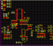
I fooled also with the layout a little and almoust all components are SMD. That means there is a very little space for the ground plane on top. On the other hand the bottom will be very rarely populated, almoust empty.
Is that a problem? I haven't got a lot of experinece with the all SMD design so I am not sure about it.
I attach this image, it does not represnet a final layout, it is just a begining to see how the things are progresing. The idea is to put everuthing (except psu) on a single 160x100mm board, less if it is posible.
Pred
Attachments
Re: I am back
That is a great solution-> people can then experiment with different kinds off inputs, without destroying the main pcb🙂
I also think, that this is the best way to do with the "third" capacitor"
Please remember a 47K resistor from "SDOUT" pin 26 to ground, this enables "Hardwaremode"
You should keep the TL431 "UR3" it´s setting the voltage at 3.3V
you can share that psu with the VDCS "U2A and U2B".
Why have you given the ferrite bead a "value" at 47uH?
Do we use the leaded versions or smd here from Farnell?
Else it´s looking very good😎
You could use the toplayer for all the connections, and the buttomlayer-> under the pcb could be a single large groundplane.
It´s fine to stick with a eurosize pcb
Please start with putting the decoupling capacitors, as close to the VSS pins at each chip. From that point, make a via directly to the groundplane.
Best regards
Kim
pred said:Hi,
I attached to this post my view on the CS receiver circuit. You will see that there is no torx on the board. I thought that including this would create a lot of problems, and since some people would like to use transformer for the SPDIF input I just left the capacitors and resitors.
In this way the choice is yours.
Pred
That is a great solution-> people can then experiment with different kinds off inputs, without destroying the main pcb🙂
pred said:
Finally, I am not sure about PSU decoupling capacitors, but since I saw that I will eventually have the place I will put the "third capacitor", most probably not SMD, with the footprint for small WIMA's (like 63V polypropilen types 5mm spacing). Please if someone has the time, look if I have not connected something wrong and I will continue, in next few days on the AD part.
I am not certain is the additional TL for the switch selector is necessary or the bead plus capacitors will do the thing?
Pred
I also think, that this is the best way to do with the "third" capacitor"
Please remember a 47K resistor from "SDOUT" pin 26 to ground, this enables "Hardwaremode"
You should keep the TL431 "UR3" it´s setting the voltage at 3.3V
you can share that psu with the VDCS "U2A and U2B".
Why have you given the ferrite bead a "value" at 47uH?
Do we use the leaded versions or smd here from Farnell?
Else it´s looking very good😎
pred said:
PCB Layout Post #61
I fooled also with the layout a little and almoust all components are SMD. That means there is a very little space for the ground plane on top. On the other hand the bottom will be very rarely populated, almoust empty.
Is that a problem? I haven't got a lot of experinece with the all SMD design so I am not sure about it.
I attach this image, it does not represnet a final layout, it is just a begining to see how the things are progresing. The idea is to put everuthing (except psu) on a single 160x100mm board, less if it is posible.
Pred
Pred
You could use the toplayer for all the connections, and the buttomlayer-> under the pcb could be a single large groundplane.
It´s fine to stick with a eurosize pcb
Please start with putting the decoupling capacitors, as close to the VSS pins at each chip. From that point, make a via directly to the groundplane.
Best regards
Kim
Re: Re: I am back
Thanks for the comments. Values for beads are unimportant. I'll change it. My problem with third capacitor is that it is furhter and further away from the chip. But I'll leave it since I will put the OSCON nearest to the chip and than gradually add capacitors in listening comparison to see if it is better.
I'll add the resistor. Beads are smd 0805 footprint.
I am not familiar that someone is usin the ground plane on the bottom, are you sure it will be ok? But I did not see people feeding with current sources the pcb's 😀
I'll change that and post tomorrow or the day after. Than we go to the AD circuit...
Pred
PS
I would be rather glad if someone joins us with more experinece on digital pcb and decoupling design, but I think they will comment if we do some cardinal sin 😉
kimschips said:
That is a great solution-> people can then experiment with different kinds off inputs, without destroying the main pcb🙂
I also think, that this is the best way to do with the "third" capacitor"
Please remember a 47K resistor from "SDOUT" pin 26 to ground, this enables "Hardwaremode"
You should keep the TL431 "UR3" it´s setting the voltage at 3.3V
you can share that psu with the VDCS "U2A and U2B".
Why have you given the ferrite bead a "value" at 47uH?
Do we use the leaded versions or smd here from Farnell?
Else it´s looking very good😎
You could use the toplayer for all the connections, and the buttomlayer-> under the pcb could be a single large groundplane.
It´s fine to stick with a eurosize pcb
Please start with putting the decoupling capacitors, as close to the VSS pins at each chip. From that point, make a via directly to the groundplane.
Best regards
Kim
Thanks for the comments. Values for beads are unimportant. I'll change it. My problem with third capacitor is that it is furhter and further away from the chip. But I'll leave it since I will put the OSCON nearest to the chip and than gradually add capacitors in listening comparison to see if it is better.
I'll add the resistor. Beads are smd 0805 footprint.
I am not familiar that someone is usin the ground plane on the bottom, are you sure it will be ok? But I did not see people feeding with current sources the pcb's 😀
I'll change that and post tomorrow or the day after. Than we go to the AD circuit...
Pred
PS
I would be rather glad if someone joins us with more experinece on digital pcb and decoupling design, but I think they will comment if we do some cardinal sin 😉
Re: Re: Re: I am back
When the components are primay smd´s then you have all the connections on top off the pcb, and not so much space for a groundplane there.
A good source is Per-Anders sjostrom he has done a lot off projects with pcb´s and smd and throught hole components
Look here:
http://home.swipnet.se/~w-50719/hifi/
Guido Tent do you have time to help us?
Best regards
Kim
pred said:
I am not familiar that someone is usin the ground plane on the bottom, are you sure it will be ok? But I did not see people feeding with current sources the pcb's 😀
I'll change that and post tomorrow or the day after. Than we go to the AD circuit...
Pred
PS
I would be rather glad if someone joins us with more experinece on digital pcb and decoupling design, but I think they will comment if we do some cardinal sin 😉
When the components are primay smd´s then you have all the connections on top off the pcb, and not so much space for a groundplane there.
A good source is Per-Anders sjostrom he has done a lot off projects with pcb´s and smd and throught hole components
Look here:
http://home.swipnet.se/~w-50719/hifi/
Guido Tent do you have time to help us?
Best regards
Kim
Re: Re: Re: Re: I am back
Hi
I usually plan all SMD on one side, and the groundplane on the other. Connect all IC grounds with a via to the plane. Connect the respective decoupling caps on the SMD layer with he IC. This way NO decoupling current runs thruogh the plane, which is the best you can achieve.
best
kimschips said:
When the components are primay smd´s then you have all the connections on top off the pcb, and not so much space for a groundplane there.
Guido Tent do you have time to help us?
Best regards
Kim
Hi
I usually plan all SMD on one side, and the groundplane on the other. Connect all IC grounds with a via to the plane. Connect the respective decoupling caps on the SMD layer with he IC. This way NO decoupling current runs thruogh the plane, which is the best you can achieve.
best
Some more on capacitors 🙂
I didn't go to lunch to read this again 😀
So I will quote from guido's article:
-------------------------
Modern electrolytics are far better RF performers. Their construction is such that the series inductance is very low (both films are terminated at the same side). They have very lowimpedance over up to 4 decades in frequency; Enough to say goodbye to the additional ceramic capacitor. It saves money and space as well and eliminates the risk of yet another resonance.
--------------------------
So this is the part that explin's it all. I think we should stick to two capacitors and that is it. One additional for those who want to add a ceramic one.
Pred
kimschips said:Have you studied Tentlabs decoupling article?
I didn't go to lunch to read this again 😀
So I will quote from guido's article:
-------------------------
Modern electrolytics are far better RF performers. Their construction is such that the series inductance is very low (both films are terminated at the same side). They have very lowimpedance over up to 4 decades in frequency; Enough to say goodbye to the additional ceramic capacitor. It saves money and space as well and eliminates the risk of yet another resonance.
--------------------------
So this is the part that explin's it all. I think we should stick to two capacitors and that is it. One additional for those who want to add a ceramic one.
Pred
Long time no see
Hi frends,
I guess you thought that I abandoned this project. Well if you did you are wrong. I always thought that the amount of bad luck is limited but I guess I was wrong
Frist I got seek from flu. Than I had my portable crash, windows decided to kill themself, fortunately I keep backups. Than an industrial partner decided that the time is to finish his ASIC, although I thought I had like two more months. Than I decided to quit smoking (after 14 years), which had an effect that I was dizy like for two weaks. If someone is asking if I am still holding on, the answer is yes 😀 , one of the (minor) reasons for quiting is more money for DIY (every 5 days I was smoking one 0.47u 630V PIO cap 😎 ). Than I again got seek from flu (viruses are really attacking me on all fronts), and started to hate students that transmit me all of this stuff .
.
Then I decided it is time to end the lows and continue the project. So here is what I did:
Hi frends,
I guess you thought that I abandoned this project. Well if you did you are wrong. I always thought that the amount of bad luck is limited but I guess I was wrong
Frist I got seek from flu. Than I had my portable crash, windows decided to kill themself, fortunately I keep backups. Than an industrial partner decided that the time is to finish his ASIC, although I thought I had like two more months. Than I decided to quit smoking (after 14 years), which had an effect that I was dizy like for two weaks. If someone is asking if I am still holding on, the answer is yes 😀 , one of the (minor) reasons for quiting is more money for DIY (every 5 days I was smoking one 0.47u 630V PIO cap 😎 ). Than I again got seek from flu (viruses are really attacking me on all fronts), and started to hate students that transmit me all of this stuff
. Then I decided it is time to end the lows and continue the project. So here is what I did:
CSreceiver
I touched up the schematics. Basically tonight I have finished all parts of the DAC board. I forgot to mentione that my Protel licence expired last week so I lost some time while we acquired new one at work.
Now I need who ever is ready to check the connections and the modes of different chips. Basically looking for bugs. I will do it in the same time so I hope that there are no errors before I start to do the layout.
CS receiver
1. I have put CS to output in I2S mode (C to one others to zero)
Attachments
AD SRC
Here there are a lot of changes:
1. There are two clocks and their corresponding clocks. For AD1896 you have to put it into the slave mode so there are additional chips.
2. For the 27MHz+ clock for the AD I predicted both CMOS clock or simple quartz since the quality is not critical
3. One can decide on the mode of operation using jumpers (slave or master)
What to look for:
1. As before look for errors and check that everuthing is correct.
2. Check is there a thing to change in order to be compatible wiht BB SRC chip, since it can work on 192k from 1 clock (some say it is wors sonicaly)
Attachments
DAC
Dac schematics are posted for the first time.
Check them for errors. Make wishes for changes. I also have jumpers in order to change the mode of opperation. In this way you can use each in mono or two in stereo in paralell.
That is it. Hope you have energy to continue.
Since I am puting most of the energy into this project I think I have a right to name the dac. Although maybe done so many times in the past I have decided to name it after my daughter Sofija (yes there is a "j" in the name, it is not an error). Hope you do not mind.
Attachments
Anytime I see a ‘4040 I can be sure the circuit will not work and this DAC is no exception. Is it considered “unmanly” to read a data sheet and do cursory min/max timing? Pred, I suggest you spend more time validating the basic circuit and less time obsessing over minutia, like ferrites and bypass caps.
I think the moderators would do everyone a favor by deleting every post and schematic that mentions or uses a ‘4040. That way, know-nothing newbies will be less likely to copy a bad design.
I think the moderators would do everyone a favor by deleting every post and schematic that mentions or uses a ‘4040. That way, know-nothing newbies will be less likely to copy a bad design.
Re: Re: Re: I am back
As examples you can check all my
SMD projects -> groundplane solderside
Holemounted projects -> groundplane component side
Gainclone, QRP-01, mainly holemounted -> groundplane solderside
SMD projects -> groundplane solderside
If you have a doublesided board you can have the groundplane on either side. Which side you choose is determined with the side you can have as much copper as possible. A "whole" groundplane is the basic goal, always. If you only have holemounted parts it doesn't matter (not much) which side because each side you choose but it can a small advantage to have it on the componentside because you can get some shielding but if you have SMD parts you want to aviod vias which you have for free if you have holemonted parts. So the rule of thumb is: Groundplane is located on the opposite side as the SMD part.pred said:I am not familiar that someone is usin the ground plane on the bottom, are you sure it will be ok? But I did not see people feeding with current sources the pcb's 😀
As examples you can check all my
SMD projects -> groundplane solderside
Holemounted projects -> groundplane component side
Gainclone, QRP-01, mainly holemounted -> groundplane solderside
SMD projects -> groundplane solderside
Ulas said:Anytime I see a ‘4040 I can be sure the circuit will not work and this DAC is no exception. Is it considered “unmanly” to read a data sheet and do cursory min/max timing? Pred, I suggest you spend more time validating the basic circuit and less time obsessing over minutia, like ferrites and bypass caps.
I think the moderators would do everyone a favor by deleting every post and schematic that mentions or uses a ‘4040. That way, know-nothing newbies will be less likely to copy a bad design.
Thank you for finding the error in writing. The idea was to put the VHC4040 which works min on 90MHz and typically on 140MHz. I think that this is fast enough.
BTW, I think that would be more productive to help us and point to the device that is faster and that you think is more suitable. Not like you do playin "god" that knows everuthing and does anything.
As yoda says "Don't propose, do!" 😉
Pred
Re: Re: Re: Re: I am back
Yes I undestood that, from guido's post. It is funny how we are slaves of our habits. I mean now it is really imbarasing that I even asked 🙄 .
Pred
peranders said:
If you have a doublesided board you can have the groundplane on either side. Which side you choose is determined with the side you can have as much copper as possible.
Yes I undestood that, from guido's post. It is funny how we are slaves of our habits. I mean now it is really imbarasing that I even asked 🙄 .
Pred
What’s your problem, Pred? You asked others to look over your design and point out the errors and that’s what I did. It’s your design and if you want to use a ‘4040, go ahead. But before you spend the money to have PCBs made, you should at least read the datasheet and understand the limitations of the chip as it could save you a lot of headaches when it comes time to debug your design.
By the way, using a VHC part will not solve the problem. Hint: It’s not the speed of the part but the maximum propagation delay from the clock to Q7 plus the setup time of the flipflop. If you ever get around to reading the datasheet, you will notice the ‘4040 clocks on the falling edge whereas the ’74 clocks on the rising edge. That means you have less than 5ns to propagate through the counter and meet the 16ns setup time of the latch.
Now, you can ignore my analysis and stick with the ‘4040, or you can do some more reading, learning, and thinking and choose an alternative. I'm not going to tell what to do: It’s your design.
Ulas said:----
Hint: It’s not the speed of the part but the maximum propagation delay from the clock to Q7 plus the setup time of the flipflop. If you ever get around to reading the datasheet, you will notice the ‘4040 clocks on the falling edge whereas the ’74 clocks on the rising edge. That means you have less than 5ns to propagate through the counter and meet the 16ns setup time of the latch.
Now, you can ignore my analysis and stick with the ‘4040, or you can do some more reading, learning, and thinking and choose an alternative. ---
= good info!
Arne K
Ulas said:What’s your problem, Pred?
By the way, using a VHC part ....
Do you really want to tell me that you do not see the difference between your first and second post? Hint: In the second one you are trying to help, while in the first you play allmighty.
Anyway thanks for the input I'll look into it...
Pred
I don’t see any difference. In my first post I told you the ‘4040 wouldn’t work and wondered why you, and others like you, don’t read the datasheets and make your own decisions. Instead, you come to the forum and expect others to make the design decisions for you, tell you what to do, and how to do it. In my second post I told you the ‘4040 wouldn’t work and suggested you read the datasheet. I should have remained silent and let you struggle to understand why your circuit didn’t work.
Pred,
The '4040 you are using to divide the clock is a ripple counter and as such the propagation delay is cummulative i.e the greater the divisor, the greater delay. Your circuit compounds that by having the '4040 and the '74 clock on opposing edges, halving your timing budget but that point is moot as the propagation delay to Q7 is nearly, if not equal to, the period of your 24 meg clock. This is a less than ideal state as the signal at the D input to the '74 has to be stable for around 6ns prior to a clock transition.
I would suggest you use the '163 synchronous counter. Not only does it have a uniform propagation delay across all 4 Q outputs it also clocks on the same edge as the '74. This means signals heading for the D input of the '74 can have a nice meal, wave to Darth Ulas and still be stable in time for the arrival of the next 24 meg rising edge.
Re: CSreceiver
This part looks fine-> no comments here🙂
Kim
pred said:Now I need who ever is ready to check the connections and the modes of different chips. Basically looking for bugs. I will do it in the same time so I hope that there are no errors before I start to do the layout.
CS receiver
1. I have put CS to output in I2S mode (C to one others to zero) [/B]
This part looks fine-> no comments here🙂
Kim
- Status
- Not open for further replies.
- Home
- Source & Line
- Digital Source
- NEW DAC project released->Please comment!!