Hi Daniel
Food for thought! I've been reading the 'Needle' thread for the past few days and there seems to be a diverse view on 'stand alone', 'sub' and notch filters assisting. So there is plenty of scope to experiment it seems.
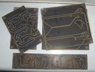
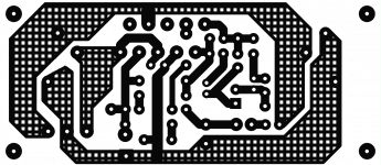
I have, once again, finalised the PCB patterns for the toner transfer.
3 PCB's -
Amplifier - 69mm x 28mm
Rectifier - 82mm x 48.5mm
Regulator - 82mm x 88mm
The rectifier and regulator will fit together face to face, spaced of course, the amplifier PCB is the final iteration before I had the slight issue with my hard drive.
Onwards and upwards!
Foo
Food for thought! I've been reading the 'Needle' thread for the past few days and there seems to be a diverse view on 'stand alone', 'sub' and notch filters assisting. So there is plenty of scope to experiment it seems.
I have, once again, finalised the PCB patterns for the toner transfer.
3 PCB's -
Amplifier - 69mm x 28mm
Rectifier - 82mm x 48.5mm
Regulator - 82mm x 88mm
The rectifier and regulator will fit together face to face, spaced of course, the amplifier PCB is the final iteration before I had the slight issue with my hard drive.
Onwards and upwards!
Foo
Attachments
Last edited:
hello there
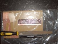
Progress!
Today I made it to the printers to get my patterns printed. As a bonus, Mark, the proprietor has a brand new 'digital' laser copier which has replaced the old photo copier.
By 'eck! It works really well to boot! Although it is hard to tell the difference between old and new visually there is a distinct tactile difference in that the new machine is printing a thicker layer of toner.
It's also bloody fast! 😀
Once home I cut some PCB blanks and using my modified laminator I transferred the toner patterns to them. Followed, of course, by etching in the ferric.
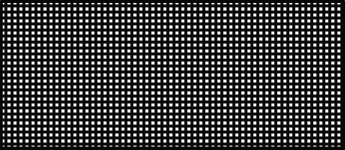
Using the 'hatched' fill effect for the traces and planes definitely paid dividends in terms of quality and reliability of the transfer. Only the smallest area needed some attention with a permanent marker on the first PCB and then I could have left it it was that minimal.
All the boards are now etched and merely require drilling and the cleaning to get rid of the toner. I am very pleased with the results and can't wait to start the build in earnest.
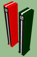
I have also been playing with colour schemes for my 'proposed' Needles. I am definitely going to build a pair for my first DIY speakers. Currently I rather fancy doing them in British racing green. Although my 'significant other' likes red, it's her favourite colour. Decisions, decisions......
I will post some better pictures of the boards tomorrow when I have better light to work by.
regards
Foo
Progress!
Today I made it to the printers to get my patterns printed. As a bonus, Mark, the proprietor has a brand new 'digital' laser copier which has replaced the old photo copier.
By 'eck! It works really well to boot! Although it is hard to tell the difference between old and new visually there is a distinct tactile difference in that the new machine is printing a thicker layer of toner.
It's also bloody fast! 😀
Once home I cut some PCB blanks and using my modified laminator I transferred the toner patterns to them. Followed, of course, by etching in the ferric.
Using the 'hatched' fill effect for the traces and planes definitely paid dividends in terms of quality and reliability of the transfer. Only the smallest area needed some attention with a permanent marker on the first PCB and then I could have left it it was that minimal.
All the boards are now etched and merely require drilling and the cleaning to get rid of the toner. I am very pleased with the results and can't wait to start the build in earnest.
I have also been playing with colour schemes for my 'proposed' Needles. I am definitely going to build a pair for my first DIY speakers. Currently I rather fancy doing them in British racing green. Although my 'significant other' likes red, it's her favourite colour. Decisions, decisions......
I will post some better pictures of the boards tomorrow when I have better light to work by.
regards
Foo
Attachments
Looks really good. You passed a milestone for sure.
Good you refresh my memory as to the reason for cross hatching?
I think I read it in a Tom Gootee article a while back.
Anyways good stuff.
Good you refresh my memory as to the reason for cross hatching?
I think I read it in a Tom Gootee article a while back.
Anyways good stuff.
Hi Globug
Cheers 😀 It's a start!
My reasoning, from experience, for cross hatching was that large solid areas of toner tend not to be very even in density and not dense enough at times. Well dense enough to do the job but at times I was having issues with slight etching of solid areas making the surface look crap with risks of weak points. There was also a higher rate of 'touching up' required at times due to 'failure to stick' of the toner.
The hatching seems to give better results in density AND fixing. I also think it looks pretty good 😎 Also a secondary benefit is to do with soldering. Large areas of copper soak a lot, relatively speaking, of the solder irons heat causing solder to spread thinly around a component lead. Hence the use of 'thermal pads' in professional PCB's. The hatch fill will work in much the same way allowing a better solder joint than in a similar solid plane of copper.
Etching PCB's is one of my favourite hobbies I think. I've only been doing my own for 2 - 3 years.
regards
Foo

Damn!
All is not well! 😱
The regulator and rectifier Boards are fine. Test fitting components shows all is well, though the diode bridges were a bit tight for pitch.
BUT! There turns out to be a problem with the amplifier PCB's. Namely the footprint for the LM3876T.............Like Pin 1 and Pin 11 being 15mm Pitch rather than the required 17.02mm of the real thing.
I dare say I could squeeze the pins in to fit but that's not for me. It does, however, explain why I couldn't seem to match the layout of the redraw to the original.
The redrawn PCB is now 69mm X 30mm.
Globug - Just a heads up on my technique for getting the hatched planes. I am using sprint layout for my PCB design. This has the facility to draw 'zones' which can be solid or hatched depending on choice.
I know some software packages can do this as a 'plane fill' automatically but in sprint you draw the outline and this is filled upon completion.
To make it easier to do I export the track pattern with the standard ground plane. This auto fills and is different from the 'Zone fill'.
I import the image into 'The Gimp' and select the ground plane and apply a Colour to Alpha instruction. Basically these areas become transparent. In sprint I then draw, the same physical size, the PCB without any trace patterns at all and draw a zone over the whole PCB.
This is exported and opened in The Gimp as a layer. This layer is copied into the first Gimp window, which has the trace pattern in it, and is placed as the bottom layer.
The only areas of this hatched plane that can be seen are those that show through the transparent areas of the trace layer. Then simply merge and save.
I hope this helps. See the 2 attached images to clarify. One is the hatched plane and the other is the trace pattern with the transparent areas done. Download them into your favourite image editor and stack them to see what I mean.
regards
Foo
Attachments
Thanks for the info.
Could you use a similar process using Google Sketchup?
The reason I ask is it is easy for me to use metric and imperial measurements on one program. Then just export a 2D graphic Jpeg?
I really like Sketchup. (And Ketchup)
Could you use a similar process using Google Sketchup?
The reason I ask is it is easy for me to use metric and imperial measurements on one program. Then just export a 2D graphic Jpeg?
I really like Sketchup. (And Ketchup)
Hi there
Sprint exports the PCB only so no surrounding empty space is present. Thus the PCB image is perfect to import into sketchup onto the face of a matching dimensioned panel. This is what I have been doing to 'proof' my layout. Of course this failed to catch my error with the LM's Pitch but I had that wrong from the start.
For other software you may just have to crop your image down to the actual PCB to prep it for import into sketchup.
I like Brown ketchup.....On a sausage sandwich of course! Sketchup is a close second 😀
regards
Fenris
Last edited:
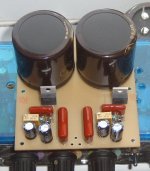
Hi Chaps
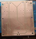
I have the Regulator PCB's fully populated. All they need is the fitting of Heat sinks to the regulator IC's.
Minor things that showed up were that the poly caps were of a smaller physical size than the data sheet indicated. This is fine of course but I could have had the regulator, the cap and the rest of the components in front of it closer together.
My 100uF caps had a pitch of 3mm the PCB was set for 5mm 😱 So an extra hole was drilled and the component lead bent over to make contact.
Other than that it's all looking good.
The rectifiers are in place on their PCB's but due to a late change in design I have to order 20 100nF caps to finish these off.
Back to heat sinks. I am wondering if cut down CPU sinks would do. The distance between the back of the 338's and the main caps is 10mm. So something in the order of 6 - 8mm is in order.
regards
Foo
PS. Just finished the second regulator, I'd forgotton to fit the electrolytic caps, It turns out The bag of 4 consisted of 3 100uF with a 3mm Pitch and 1 with the, correct, 5mm Pitch. Naughty Rapidonline!
Attachments
Last edited:
Hi there
Between Now and getting the new prints of the corrected Amplifier PCB done I am reading up on Heat sinks.
Using Rod Elliots, free download, Heat sink calculator it appears my heat sink has a thermal rating of 1.11C/W. This an approximation, Rod advises, but is a good starting point.
Another site uses the equation -
50/SqrRt of the surface area (exposed) In my case 1197Cm2 which comes out at 1.45C/W
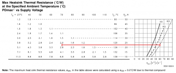
Looking at the data sheet for the LM3876T It looks like at +/-30VDC with an 8ohm load I will be looking at 42W OP. Taking this to the Power dissipation VS Output Power suggest a PD of around 33W.
Then referencing this to the max heat sink Thermal resistance at Specified Ambient temp It looks like for an ambient temp of 25C a Thermal rating of 5.1 is needed. SO the allow headroom A smaller thermal rating is needed. 1.2 would see me good for 90C which will never happen in the UK 😀
So I thinking of cutting the heat sink in 2 to allow a different enclosure layout. This would take the Thermal rating of each half to 2C/W Which will be good for an ambient temp of 70C.....Still not going to happen in the UK 😀
If I get this bit right - Thermal resistance X OP +25C Ta as a base would give me 1.11C/W x 33W PD + 25C = 62C X 2 for both IC's on the same sink 123C. Absolute maximum rating for the IC's is 265C So I have half again head room?
For the 2C/W with one IC I would be looking at 91C So again still well under the maximum temp?
Have I understood the above well enough to be correct?
regards
Foo
PS keep it simple please I am horrendous at math. 🙁
Between Now and getting the new prints of the corrected Amplifier PCB done I am reading up on Heat sinks.
Using Rod Elliots, free download, Heat sink calculator it appears my heat sink has a thermal rating of 1.11C/W. This an approximation, Rod advises, but is a good starting point.
Another site uses the equation -
50/SqrRt of the surface area (exposed) In my case 1197Cm2 which comes out at 1.45C/W
Looking at the data sheet for the LM3876T It looks like at +/-30VDC with an 8ohm load I will be looking at 42W OP. Taking this to the Power dissipation VS Output Power suggest a PD of around 33W.
Then referencing this to the max heat sink Thermal resistance at Specified Ambient temp It looks like for an ambient temp of 25C a Thermal rating of 5.1 is needed. SO the allow headroom A smaller thermal rating is needed. 1.2 would see me good for 90C which will never happen in the UK 😀
So I thinking of cutting the heat sink in 2 to allow a different enclosure layout. This would take the Thermal rating of each half to 2C/W Which will be good for an ambient temp of 70C.....Still not going to happen in the UK 😀
If I get this bit right - Thermal resistance X OP +25C Ta as a base would give me 1.11C/W x 33W PD + 25C = 62C X 2 for both IC's on the same sink 123C. Absolute maximum rating for the IC's is 265C So I have half again head room?
For the 2C/W with one IC I would be looking at 91C So again still well under the maximum temp?
Have I understood the above well enough to be correct?
regards
Foo
PS keep it simple please I am horrendous at math. 🙁
I recommend using the graph that National show in the 3886 datasheet.
Does the 3876 have the same design graph?
Then double the sink rating from what National says you need.
Other than dividing by 2 there is no other arithmetic.
Does the 3876 have the same design graph?
Then double the sink rating from what National says you need.
Other than dividing by 2 there is no other arithmetic.
I would go all the way to the left temperature value Ta that your heatsink/s may experirnce in normal operation.
For external heatsinks in the UK 25degC to 30degC is a normal maximum.
For internal heatsinks in the UK allow 40degC to 50degC.
Let's suppose you use external sink and Ta <=25degC.
You would extract somewhere between 3.8C/W and 5.1C/W. Let's guess at 4.4C/W.
Doubling comes to 2.2C/W for each chipamp.
For a stereo pair you should use 1.1C/W
The reason I don't use 70degC nor anything higher is that the chip will run hot. So hot that the protection systems will do their best to prevent damage to the chipamp. That means triggering of the protection circuits. That does not sound nice.
Last edited:
Hi Andrew
Thanks for catching my 'errored thinking'. It seems I've been misunderstanding Thermal rating for quite some time..
I'm now trying to check I have rated my heat sink correctly as there is a little ambiguity with the data input.
Off to the printers on Monday to get my corrected Amplifier PCB done.
regards
Foo
Here's the considerations:
1). The thermal dissipation size of a big sheet of aluminum is fantastic, but the thermal interface speed is insufficient.
2). The thermal interface speed of a thick chunk of aluminum is fantastic, but the thermal dissipation size is insufficient.
Neither case 1 nor case 2 will work as an heat sink.
But thermal pasted and bolted together they can work.
Your enclosure is at case 1. So, add a nice big thick heat spreader, so easily available as bar stock from the hardware store. 🙂
And you might want some sort of thermally efficient decoration, such as U-channel onto the sides of the enclosure.
Many homebrew heat sinks are successful, but you need speed and size and ventilation.
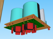
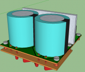
Hi Daniel
Thermal compound or Sil-Pads will be used never fear.
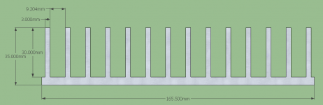
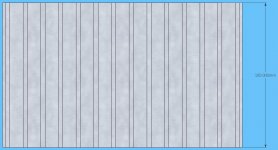
The enclosure situation is a very amorphous part of the build to which end I have purchased a large heat sink to use directly with the chips.
As you can see in the drawings it is a fairly sizable chunk of extruded Ali'.
It may well get cut in half along it's widest measure to allow a shallower enclosure but until I am sure I have actually worked out it's thermal rating I'm not sure what's happening.
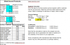
See also the ESP heat sink calculator screen shot. I think I have the correct measures in the correct places.
regards
Foo
Thermal compound or Sil-Pads will be used never fear.
The enclosure situation is a very amorphous part of the build to which end I have purchased a large heat sink to use directly with the chips.
As you can see in the drawings it is a fairly sizable chunk of extruded Ali'.
It may well get cut in half along it's widest measure to allow a shallower enclosure but until I am sure I have actually worked out it's thermal rating I'm not sure what's happening.
See also the ESP heat sink calculator screen shot. I think I have the correct measures in the correct places.
regards
Foo
Attachments
That 5mm backplate will allow two devices to run hot at their contact/interface locations, but leave the extremities of the sink relatively cool. This will increase Tc to above the predicted temperature.
Note that ESP does not ask for number of devices/locations, nor the thicknesses of fins & backplate.
What's the plural of thickness?
Note that ESP does not ask for number of devices/locations, nor the thicknesses of fins & backplate.
What's the plural of thickness?
Last edited:
Hi there
Andrew - Rods site does indicate that the actual math is more involved and the spread sheet is merely a 'rough guide'. For those with experience I'm sure it's enough.
I think the plural is Thicknesses. 🙂
Daniel - Enough for 1.................. Oh..... FIDDLE!
But both of you indeed indicate it's not enough for the job of both chips.
I have a CPU Sink. Although I understand this may be no good due to the density of the fins designed as the are for forced air flow. But it is 70mm x 82mm x 30mm High. There are 28 fins which are 25mm high. The base is 7mm thick near the centre section and thins out towards the edges to 3mm. The surface area is 1246.4cm^2.
Would this be any good? Failing that could one of you wise gentlemen point me at a known heat sink.
regards
Foo..... The aghast!
- Status
- Not open for further replies.
- Home
- Amplifiers
- Chip Amps
- New amplifier...possibly..