Someone commented on bypassing R10 with a 100pF cap. That makes this amp go ballistic. I have it bypassed with a 15 pF cap, and even that is a little borderline.
Well, it was only a suggestion ...

R10 is your feedback resistor, ya? (or did I miss the real one?)
The new cap may have been coupling up with C20 ... you may need to tinker with both.
What frequency does is oscillate at? You want to tune your feedback to bring that frequency down by about 3db, to gain some stability.
Someone commented on bypassing R10 with a 100pF cap. That makes this amp go ballistic. I have it bypassed with a 15 pF cap, and even that is a little borderline.
Lead compensation is more effective if taken from the output of the VAS, not the output of the amplifier. You don’t want the phase shift of the output stage added in. When doing this it also linearizes the VAS and lowers it’s output impedance at high frequency - which makes the whole output stage more stable in addition to providing loop stability Set the pole frequency between that cap and R10 to be about half the frequency of oscillation. If you’re oscillating at say 300kHz, set the pole (causing a zero in the loop gain) to 150k. The fact that making the cap too big causes massive oscillation means you’re fiddling in the right spot. If you get this right you may be able to remove other band aids in the circuit.
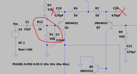
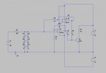
I think it's close. I really appreciate the help with this. Attached is an updated schematic as it stands right now. For the most part, it's great.
There is a residual oscillation at 8.33 MHz, which gets much worse (though the frequency changes little if any) when a 1 nF cap is clipped across the output. The frequency involved makes me wonder if the output stage itself is oscillating. Ideas?
Removing C19 and C20 made things worse.
There is a residual oscillation at 8.33 MHz, which gets much worse (though the frequency changes little if any) when a 1 nF cap is clipped across the output. The frequency involved makes me wonder if the output stage itself is oscillating. Ideas?
Removing C19 and C20 made things worse.
Attachments
I think it's close.
Have you tried disconnecting R20 from the junction of D5 and D6, going straight to the output instead? In fact you may want a bit of resistance between that junction and the output.
Another suggestion as you follow my first one (try there 2.2k instead 330R - it will decrease the first stage load):
Try to connect the led D3 cathode to the junction of emitter Q14 and resistor R16 and decrease R17. May be you need to adjust R15 and R16 values as you will have polarization and poles changes. It will give you less distortion and better frequency response.
It was a work of Hawksford.
If you use KSC1845 instead of BD139 in position Q14 you will have lots of advantages (Better Ft, lower capacitances, better Hfe behavior and value).
Try to keep all compensation caps as low as possible. My SIM showed little oscillation in square wave test after all changes, so you will need to work around it in your real amplifier.
Regards
Last edited:
Interesting note: a 10 nF cap across the output stops the oscillation. This is odd, as I would have expected it to make things worse, not better given that a 1 nF cap makes it go nuts. I've never heard of an amp with a small cap permanently across the output, which makes me suspect that there is a reason why it would be a bad idea, but interesting none the less.
In the simulation I ran I'd have to say that it all seemed pretty stable. I couldn't provoke oscillation even with capacitive loading, all of which makes me wonder if your issues are layout related.
One thing I would look at though is that input arrangement. Those 470pF caps make me nervous 😀
Try something like this.
One thing I would look at though is that input arrangement. Those 470pF caps make me nervous 😀
Try something like this.
Attachments
The only things I’ve ever needed to make/keep amplifiers like this stable are a small Miller cap on the VAS, an experimentally tuned in lead compensation cap (from VAS output to the summing node), and the RF short across the input (Mooly’s post). Even with point to point wiring on a perf board and 6” long leads to output devices on heat sinks. And of course bypass caps, connected near where the high current is drawn, and returned separately from low current ground paths. If they are in the wrong physical place they become useless. Capacitive-load-induced issues are separate, and need to be worked with the zobel and/or damped inductor in series. And sometimes the latter takes different values than you may be used to if you’re using triples or massively parallel stages. Even then the only time I’ve resorted to using base stoppers is with more than 3 outputs in parallel. if you’ve ever built RF amplifiers you’ll understand why on that one (needed if you put anything in parallel or it will push-pull oscillate).
Mooly, you are using too high gain in your simulation. R9 is 5k, not 500 ohms.
With 5k simulation shows very marginal stability. This can be fixed by removing C19 and C20 as Mooly suggests, and increasing input emitter resistors R4 and R7 to 150...220 ohms.
With 5k simulation shows very marginal stability. This can be fixed by removing C19 and C20 as Mooly suggests, and increasing input emitter resistors R4 and R7 to 150...220 ohms.
Oh, well spotted 🙂 That was a carry over from the Doug Self Blameless I modified this sim to fit.
Yes that will make a big difference...
Yes that will make a big difference...
Its usually the VAS capacitor that needs increasing to get rid of oscillation.
If the output has driver transistors into outputs then sometimes a 10R in series with output base is required to degenerate a bit.
As in all amps keep feedback path as short as possible, remember 1mm of pcb track = 1nH
If the output has driver transistors into outputs then sometimes a 10R in series with output base is required to degenerate a bit.
As in all amps keep feedback path as short as possible, remember 1mm of pcb track = 1nH
I have .1uF decoupling capacitors as close to the outputs as possible as well as 15 ohm base stoppers on the outputs. None of this has solved the problem.
I will try emp's suggestions when I have a chance.
I will try emp's suggestions when I have a chance.
The only thing that looks strange to me is c19/20.
I would have thought C20 causes a phase shift in feedback and causes some oscillation.
A quick check would be lifting one leg.
I would have thought C20 causes a phase shift in feedback and causes some oscillation.
A quick check would be lifting one leg.
Interesting note: a 10 nF cap across the output stops the oscillation. This is odd, as I would have expected it to make things worse, not better given that a 1 nF cap makes it go nuts. I've never heard of an amp with a small cap permanently across the output, which makes me suspect that there is a reason why it would be a bad idea, but interesting none the less.
With emitter followers there is always a range of pure capacitance that will make it unstable. With 3 terminal voltage regulators, they recommend a large enough output cap to swamp out anything which might be connected. No capacitance is fine, 10uf is fine, but anything in between you roll the bones. What is typical of audio amps is to put a zobel which provides for a high frequency load, and then a damped inductor in series to isolate any load capacitance (ie, 100 feet of zip cord). Many times you can get away without either. Sometimes you need it all.
The only thing that looks strange to me is c19/20.
I would have thought C20 causes a phase shift in feedback and causes some oscillation.
A quick check would be lifting one leg.
C19/C20 is a band aid for not having an RF short at the input. It is effectively shorting the differential Input at RF, but not in a good place. What you want is to provide a very low source impedance to the amplifier at infinite frequency, to push any non-dominant poles caused by the input stage higher in frequency (the frequency is dependent on the source impedance - analyze the pole/zero plot of the diff pair itself and see).
With emitter followers there is always a range of pure capacitance that will make it unstable. With 3 terminal voltage regulators, they recommend a large enough output cap to swamp out anything which might be connected. No capacitance is fine, 10uf is fine, but anything in between you roll the bones. What is typical of audio amps is to put a zobel which provides for a high frequency load, and then a damped inductor in series to isolate any load capacitance (ie, 100 feet of zip cord). Many times you can get away without either. Sometimes you need it all.
I do currently have a zobel network and a damped output inductor on this amp, and I notice some residual oscillation into no load, so I don't expect that increasing the size of the output inductor would do a whole lot.
I'll try the RF short on the input- I'd forgotten about that when designing this amp. The suggestion of increasing the emitter degeneration resistors on the input pair is also going to be something I try.
Ok, so increasing the emitter degeneration resistors on the IPS to 240 ohms took care of the majority of the issues. The RF short on the input did relatively little. It is now pretty well-behaved, for the most part.
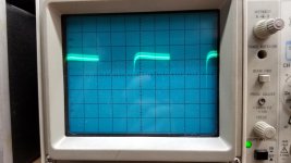
There is, however an annoying oscillation around 5 MHz on the top of the waveform at a very specific output level (relatively close to clipping) that I can't seem to get rid of. You can see it on the square wave in the attached oscilloscope image. It is only on the top part of the waveform, and the oscillation is probably about a volt peak-to-peak.
There is, however an annoying oscillation around 5 MHz on the top of the waveform at a very specific output level (relatively close to clipping) that I can't seem to get rid of. You can see it on the square wave in the attached oscilloscope image. It is only on the top part of the waveform, and the oscillation is probably about a volt peak-to-peak.
Attachments
Okay, this one was a real pain to deal with, but I think I got it nixed. First, it seems as though I made some bonehead mistakes in my initial simulation. As such, loop stability was not what it should have been. This however did not deal with the parasitic near clipping.
After many hours of testing I eliminated Q15, which took care the problem all together. In simulations, the cascode was a relatively minor performance improvement, so I am more than happy to get rid of the thing. It will remain in the new PCB layout in case I want to experiment with it, but I don't plan on using it. I will now be looking to see how many of the band-aid fixes I added can now be removed.
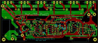
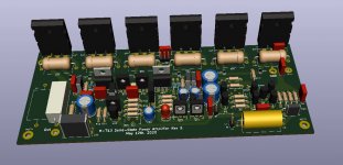
Also attached is a new PCB layout. I added a 3rd set of output devices, just for funsies. If populated, it will probably be necessary to change the drivers to 2SC4381 and 2SA1667. The PCB is now 172 x 75 mm, making it more friendly for use in a 2U chassis (something that most people probably don't care about). PCB layout critiques are appreciated, as my experience with PCB layout is relatively minimal. I tried to keep the high current loop as small as possible, and also tried to minimize the amount of stuff inside that loop.
Base stoppers are 1206 SMD parts. I believe that they will be fine. While in theory the power dissipation may be exceeded, this is an audio amplifier, not a power supply, and I expect that they will be fine even under heavy loads. They are extremely convenient from a layout perspective as well.
Also attached is the speaker protection circuit and a (still in progress) output short protection circuit. This amplifier will ultimately be digitally controlled using a microcontroller. The DC protection will operate independently, (though the microcontroller will know when the DC circuit has been triggered so the amp will stay in fault mode until manually reset). The microcontroller will also handle levels, mutes and overtemp protection. This part has yet to be designed.
While digital control is completely unnecessary for an amplifier like this it does have some interesting advantages and should be a fun project.
I appreciate all the advice that has been given, it has been a huge help.
After many hours of testing I eliminated Q15, which took care the problem all together. In simulations, the cascode was a relatively minor performance improvement, so I am more than happy to get rid of the thing. It will remain in the new PCB layout in case I want to experiment with it, but I don't plan on using it. I will now be looking to see how many of the band-aid fixes I added can now be removed.
Also attached is a new PCB layout. I added a 3rd set of output devices, just for funsies. If populated, it will probably be necessary to change the drivers to 2SC4381 and 2SA1667. The PCB is now 172 x 75 mm, making it more friendly for use in a 2U chassis (something that most people probably don't care about). PCB layout critiques are appreciated, as my experience with PCB layout is relatively minimal. I tried to keep the high current loop as small as possible, and also tried to minimize the amount of stuff inside that loop.
Base stoppers are 1206 SMD parts. I believe that they will be fine. While in theory the power dissipation may be exceeded, this is an audio amplifier, not a power supply, and I expect that they will be fine even under heavy loads. They are extremely convenient from a layout perspective as well.
Also attached is the speaker protection circuit and a (still in progress) output short protection circuit. This amplifier will ultimately be digitally controlled using a microcontroller. The DC protection will operate independently, (though the microcontroller will know when the DC circuit has been triggered so the amp will stay in fault mode until manually reset). The microcontroller will also handle levels, mutes and overtemp protection. This part has yet to be designed.
While digital control is completely unnecessary for an amplifier like this it does have some interesting advantages and should be a fun project.
I appreciate all the advice that has been given, it has been a huge help.
Attachments


- Home
- Amplifiers
- Solid State
- New Amplifier Build Stability