Thanks Andrew T. this is of great educational value to me.
see my last revision, not sure what resistor value i could use as emitter resistor for q5.
To low and it won't have any effect, to high and gain will reduce to much.
Any idea's how to determine a correct value?
Thanks Archer out............................!
see my last revision, not sure what resistor value i could use as emitter resistor for q5.
To low and it won't have any effect, to high and gain will reduce to much.
Any idea's how to determine a correct value?
Thanks Archer out............................!
Attachments
22r will do meantime. You can simulate with different, but similar, values later when you learn how to control stability. The important thing is the extra pads on the PCB.
Now do the same modifications to post8 and try R14=470r or 560r.
Add a voltage probe across the LTP collectors. What value of trim pot is required to reduce difference in collector voltage to <1uV?
Now do the same modifications to post8 and try R14=470r or 560r.
Add a voltage probe across the LTP collectors. What value of trim pot is required to reduce difference in collector voltage to <1uV?
Last edited:
for a bit of homework look up quasi complementary and search for Shaw, Baxandall and John Linsley Hood. You will find you have Baxandall's version.
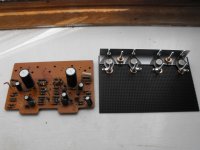
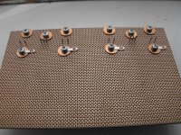
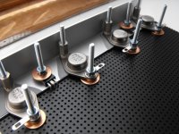
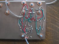
Recent progress, mounted the original 2SD292 transistors on a heatsink and this will be mounted to the alluminium chassis.
Had no TO66 silicon pads so i cut some myself.
Made Very specific HFE selections, i chose only the highest one's and mached them acooarding application in the circuit.
the tiny BD139 in the middle will be the VBE multiplier.
Also made a photo with the original circuit board next to the new one.
Greets Captain archer out........................!
Attachments

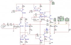
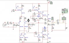
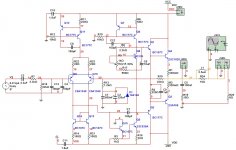
I have a question, the cap in the feedback loop is sometime's drawn with the positive terminal to the ground and sometime's like i did in the schematic below.
now this confuses me, in about 50% of the times the cap is mounted one way and 50% the other way.
I simulated that this point is 113.7mv positive with no input signal, so this would indicate that i should mount the cap with the positive lead to the base of the LTP.
But why is it sometimes inverted.
i do not have a bipolar cap in my parts-box and making one with two caps doesnt seem right to me, so can somebody help me with this
Greets captain archer out............................!!!!
Attachments
You might find Q11 needs a 100pf/220pf from collector to base.
I built a quasi that was similar and that needed the extra capacitor for stability.
I was getting some oscilation on the output.
I built a quasi that was similar and that needed the extra capacitor for stability.
I was getting some oscilation on the output.
ok thanks for the info. will simulate that, but do you know why the cap in the feedback loop is sometime's inverted with positive lead to ground and vice versa.
My first, off-the-cuff response is that which way it "should" be connected is a tossup, depending on whether the actual voltage at that node ends up slightly positive or slightly negative. But then I thought about it.
Analyzing the circuit a little deeper, a (rather small) base current comes out of Q9 and goes to ground through R18. This causes a slightly positive voltage drop across R18, and the base of Q9 is at that voltage. The overall negative feedback forces Q10's base to be that same slightly positive voltage.
On a related note - going through the thread, I noticed the suggestion in post#11 to make the input and feedback resistors the same, giving them (ignoring tolerances) the same voltage drop, setting the no-signal output to zero.
If the differential pair Q9 and Q10 were instead NPN transistors, the base currents would be going into the bases, causing a negative drop across the input resistor R18, putting a negative voltage on the base of Q9, which would show up at the base of Q10. So amps with PNP differential inputs should have the negative lead of the capacitor connected to the base.
But I don't like this design as it puts such a low voltage (less that one volt) across an electrolytic capacitor (run a simulation with signal - the voltage across the cap shouldn't change much at anything below clipping). Even capacitor manufacturers say not to do that, as it causes reduced capacitor life, as opposed to being operated near it's max voltage rating (the reccomendation I recall is to operate an electrolytic at at least 50 percent of its working voltage rating). There's also the worry of an electrolytic having greater distortion with such a low DC bias. The main solution I've seen is biasing, using two "back-to-back" caps of twice the value in series and tie their connection through a largish resistor to a voltage source (which in this case should be free of ripple and noise, as it goes straight to the amp's input). It's a "minor" thing, the cap as-is will probably contribute a lot less distortion than other things (and the simulator won't show its distortion it without some fancy model of a real-life cap), but it's something to know about.
I have a question, the cap in the feedback loop is sometime's drawn with the positive terminal to the ground and sometime's like i did in the schematic below.
now this confuses me, in about 50% of the times the cap is mounted one way and 50% the other way.
I simulated that this point is 113.7mv positive with no input signal, so this would indicate that i should mount the cap with the positive lead to the base of the LTP.
But why is it sometimes inverted.
i do not have a bipolar cap in my parts-box and making one with two caps doesnt seem right to me, so can somebody help me with this
Greets captain archer out............................!!!!
I have come across exactly the same issue... not just the feedback cap but input electroylitics too... and that was on published diagrams from the most highly regarded designers.
The voltage is only a few 10's of mv worst case, should be less if all is balanced correctly, so the best answer is measure across it when it's working and align the polarity accordingly.
alright thanks guys, will find a solution (maybe socket the cap and use a 4v or 6.3v).
the simulation showed that at full signal output the ac voltage across the cap is about 700mv or so and the dc variation is between 220 and 120 mv.
greets captain out.............................!!!
the simulation showed that at full signal output the ac voltage across the cap is about 700mv or so and the dc variation is between 220 and 120 mv.
greets captain out.............................!!!
alright thanks guys, will find a solution (maybe socket the cap and use a 4v or 6.3v).
the simulation showed that at full signal output the ac voltage across the cap is about 700mv or so and the dc variation is between 220 and 120 mv.
greets captain out.............................!!!
If the AC voltage is 700mv perhaps your test frequency is to low. That's a huge amount. What frequency are you simulating at ?
I am simulating with 1v input and 1khz sine wave
outup voltage = ~11.8v AC and voltage on the base of q10 = ~614mv AC
DC offset = ~2.3mv DC with no input signal.
voltage on the base of q10 with no input signal applied= +113mv
greets captain out...........................!!
outup voltage = ~11.8v AC and voltage on the base of q10 = ~614mv AC
DC offset = ~2.3mv DC with no input signal.
voltage on the base of q10 with no input signal applied= +113mv
greets captain out...........................!!
the orientation of the electrolytic is down to whether the amp uses PNP or NPN in the LTP.
Let's follow the quiescent current (no signal) through the LTP>
Start at j30. Current passes r22 then q9 then q14. Some of the emitter current through q9 goes via the base and not the collector. This base current continues it's journey to j22 and through r18 to signal ground. Since the (conventional) current flows from j30 via j16 and j22 to SG then all these junctions must be +ve with respect to SG.
If you know the values of the currents and the values of the resistors you can calculate the typical voltages found at all of the junctions.
I started on the left side since it is slightly simpler to see the current route.
Exactly the same route applies to flows down the right hand side of the LTP.
J30 r23 j27 q12 j20 (base current) r15, j31. All of these junctions are +ve relative to j31. J31 is the amplifier output and the amp tries to make this as close as it's able, equal to zero volts relative to audio ground.
Let's put some numbers in.
Ir11 ~3mA
Ir23 ~1.5mA
Ir15 ~1.5mA/hFE ~5uA. Assume that output offset is zero mVdc.
Vj31 =0V
Vj20 =5u * 22k = 110mV
Vj27 ~110m + 600m ~710mV
Vj30~ 1.5m * 22r + 710m ~743mV
Since we normally assume the leakage through C2 is zero, then it follows that zero current flows through R13. Vr13 =0mV
Voltage across C2 is +110mV.
If you go back through the calculations you will find that this polarising voltage across the electrolytic is dependent on hFE of the LTP pair and it also dependent on Vbe of the LTP pair.
Low gain transistors will give rise to higher polarising voltages.
Mismatched Vbe will give rise to output offset.
Next you superimpose the signal voltage (AC) on the polarising voltage to see what the total voltage is across any component.
The AC voltage across the NFB electrolytic should be near zero mVac for ALL frequencies.
If you cannot do these type of mental exercises, you are not ready to ask a simulator the right questions.
Last edited:
for a BJT input LTP the polarising voltage across the NFB capacitor is usually >60mVdc and sometimes as high as 500mVdc.The voltage is only a few 10's of mv worst case,
What Captain Archer I think is referring to is this. Here is the same amp (we all know it... the blameless class B). Look at the input cap.
Which is correct 🙂
This is why you must measure things for yourself and don't take everything on blind trust.
Edit... Both are by the designer (D Self). The first is from his audio power handbook and the second from his notes and circuit that accompanied the official PCB's for the amp.
Which is correct 🙂
This is why you must measure things for yourself and don't take everything on blind trust.
Edit... Both are by the designer (D Self). The first is from his audio power handbook and the second from his notes and circuit that accompanied the official PCB's for the amp.
Attachments

Last edited:
i shall measure the voltage at those points (when the amp is complete) and decide witch way the capacitor should be placed.
for the time being the input cap is a WIMA 3.3uf so this has no polarity but the feedback cap will be socketed so i can switch and turn the caps around.
Thanks guys.
Archer out...................!!
for the time being the input cap is a WIMA 3.3uf so this has no polarity but the feedback cap will be socketed so i can switch and turn the caps around.
Thanks guys.
Archer out...................!!
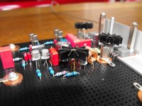
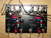
Yeeeeaaaaahh one channel working perfectly.
First there was very heavy oscillation (i loudly heard the 5 oclock local news😀) but after adding a 100pf capacitor to the vas current source all oscillations disapreared.🙂
the final schematic actualy became a bit different from the original.
The output transistors changed into 2SC1826 and 2SA768 from Sanken.
luckally i didnt solder the TO66 devices i only mounted them.
Other changes where the vas is buffered now like in the blameless amp from Douglas Self......well actually the whole amp is almost a mini blameless.
Haven't measured the offset yet but will do so soon.
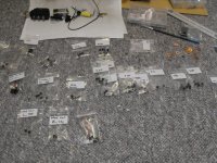
other devices are
Input 2SA1394
Current Mirror BC107C
Current Source and Vas Source BC177C
Vas 2SC538A
Vas Buffer BC107C
Output Drivers also the old BC107C BC177C
Output 2SC1826 and 2SA768
Included some pictures and DataSheets.
So lets build a identical copy and all should be fine.
Greets Captain out...........................!!!!!
First there was very heavy oscillation (i loudly heard the 5 oclock local news😀) but after adding a 100pf capacitor to the vas current source all oscillations disapreared.🙂
the final schematic actualy became a bit different from the original.
The output transistors changed into 2SC1826 and 2SA768 from Sanken.
luckally i didnt solder the TO66 devices i only mounted them.
Other changes where the vas is buffered now like in the blameless amp from Douglas Self......well actually the whole amp is almost a mini blameless.
Haven't measured the offset yet but will do so soon.
other devices are
Input 2SA1394
Current Mirror BC107C
Current Source and Vas Source BC177C
Vas 2SC538A
Vas Buffer BC107C
Output Drivers also the old BC107C BC177C
Output 2SC1826 and 2SA768
Included some pictures and DataSheets.
So lets build a identical copy and all should be fine.
Greets Captain out...........................!!!!!
Attachments
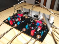
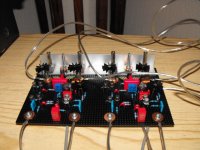
Got the second channel working.
I also added 1.8uf sibatit multilayer capacitors on the + and - V as bypass caps.
I encountered oscillations again when i used long power supply cables, but that is all gone now.
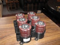
I currently have it in a test setup with a 75VA 2x15v ac power supply rectified and buffered by 2x 6800uf at 50v but the power supply caps will be 6x 4700uf at 80v in the final amp.
I found a army dump shop who sells these caps for 2 euro so lets say 3$.
and they are the Nichi Chemicon LXG long life series so thats a bargain.
And the sound, whell lets say i have never heard so much detail in a small little amplifier.
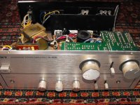
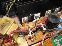
I compared it to a Sony TA-1630 wich has a similar setup inside, it is a retro amp wich included a long tailed pair as input and almost the same output transistors and a 75VA transformer.
but what a difference the sony lacks low end and is harsh in the mid range and this little amp is so clean in the high range and has a deep controlled low end.
So the final thing to do is to build it into a chassis and i aim it to be as flat as possible becouse the amps became so flat anyway but thats something for later on.
I want to thank all you guys for helping me
Included some pics of the Test setup and the sony amp as well.
Greets captain archer ou.......................!!
I also added 1.8uf sibatit multilayer capacitors on the + and - V as bypass caps.
I encountered oscillations again when i used long power supply cables, but that is all gone now.
I currently have it in a test setup with a 75VA 2x15v ac power supply rectified and buffered by 2x 6800uf at 50v but the power supply caps will be 6x 4700uf at 80v in the final amp.
I found a army dump shop who sells these caps for 2 euro so lets say 3$.
and they are the Nichi Chemicon LXG long life series so thats a bargain.
And the sound, whell lets say i have never heard so much detail in a small little amplifier.
I compared it to a Sony TA-1630 wich has a similar setup inside, it is a retro amp wich included a long tailed pair as input and almost the same output transistors and a 75VA transformer.
but what a difference the sony lacks low end and is harsh in the mid range and this little amp is so clean in the high range and has a deep controlled low end.
So the final thing to do is to build it into a chassis and i aim it to be as flat as possible becouse the amps became so flat anyway but thats something for later on.
I want to thank all you guys for helping me
Included some pics of the Test setup and the sony amp as well.
Greets captain archer ou.......................!!
Attachments

- Status
- Not open for further replies.
- Home
- Amplifiers
- Solid State
- New amp question