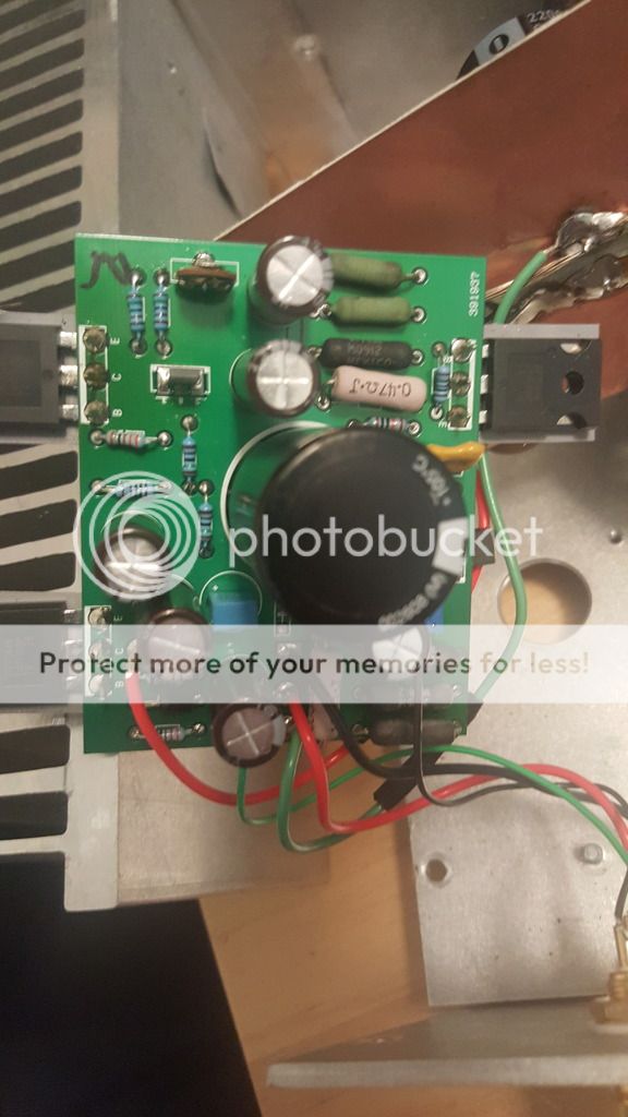
Following the resistors up from the bottom green, green, black (thats the technical term for you newbies) they all measure 0.8 if i am doing correctly.
On the circuit diagram you show R5 where is that in the actual board
On the circuit diagram you show R5 where is that in the actual board
If you consider this your chosen hobby, read Zen 7, Zen 8, and Zen 9 articles.
Try and understand the operation of this amp espescially how the bias is set and adjusted on the jfet.
Also understand the operation of the current source.
The current source should be limiting current to a sensible level, so I think I would start looking at all the components which control the current source.
A lab power supply with current limiting is also very useful, in these situations.
Last edited:
Following the resistors up from the bottom green, green, black (thats the technical term for you newbies) they all measure 0.8 if i am doing correctly.
Your measuring the total effective resistance of the parallel resistor network, so they should measure the same.
Calculate whether that is the correct value.
I am a novice that believes in miracles if that helps. And didn't everyone begin as a novice at some point.
First step if something go too hot.
Don't remplace resistors for the new ones but find why they burn ?
If not you are back to the same situation and new one cook burn again.
Is not easy to probe for novice with the power on some times is lethal danger.
Better you make short electric contact and smell magic smoke of precious transistors but you stay alive !
Take care and avoid danger

 of fire and electric shock
 servicing amplifiers is not " the game ".
I am totaly serious

Thanks soundhappy im ok with all that sort of thing I have worked around it in other areas. I won't kill myself, promise.
picodumbs your last two replies tell me its a bigger problem than I am going to be able to solve i think.
picodumbs your last two replies tell me its a bigger problem than I am going to be able to solve i think.
Turn the pcb over and take a nice close hi resolution shot of the solder joints.
One of the components may be shorted.
One of the components may be shorted.
Despite the fact, that I don't believe in miracles, the miracle is here:
This community. 🙂
I would also curious to the other side.
This community. 🙂
I would also curious to the other side.
Carefully look at the small to92 bipolar transistor to see if the solder joints are shorting out the pins.
Aaah bugger it, just replace the bipolar transistor anyway.
Remove any excess solder using solder wick, and a soldering iron.
Aaah bugger it, just replace the bipolar transistor anyway.
Remove any excess solder using solder wick, and a soldering iron.
Last edited:
Thanks soundhappy im ok with all that sort of thing I have worked around it in other areas. I won't kill myself, promise.
I know you are OK with safety. Thanks Russell66!
We don't destroy this time your nice pair of speakers hahaha.
Good news without any power on
you can compare components with the other good board visualy.
Study video tutorials about electronic basic : passive components , semiconductors, how build power supply for class A amplifiers, heat dissipation , what adequate wires diameter for the circuit, what is good solder joint ,
how test your amplifier with the multimeter , bias and offset etc.
Is not rocket science but must be

When I trying to repair something, and I have a bad and a working one, I compare resistances at the same points in when switched off.
It can reveal, where the error is.
Near semiconductors I swap the measuring leads' polarity.
It can reveal, where the error is.
Near semiconductors I swap the measuring leads' polarity.
FETs and JFETs can be tricky, because electric charge of your body can switch them. Mostly out of circuit of course.
What's the voltage across the resistors that are getting hot? (They're all in parallel, so you can just measure any one of them.)
Also, what's the voltage across the one at the bottom which is also discoloured? (You should read about 21V here.)
You could also check the voltages on the JFET (the small transistor hanging off the board just below the smoking resistors). You should get about 3.5V at the D, and about 1.1V at the S.
Report back with results.
(BTW, Nelson posted the F3 schematic and some other good stuff here: Pictures of a >>GENUINE<< Lovoltech LU1014D Wanted!)
Thanks JeffYoung,
I somehow missed it, there are important information about F3.
I will get some hi res shots of the circuit board later. I have studied it under magnification and to my eyes i can not see anything glaringly wrong.
I can see the center pin on one Jfet may need more solder but the contact still looks ok.
Now 2 things have occurred to me
1. I have 4 of these boards in total, one or two had this issue previously, now two more have the issue one could be the same board but the other is not. Which means at least three out of the four boards has the fault. To me it would be unlikely that it is a solder joint unless of course you could get a faulty batch of solder. It more points to a component fault or a design fault. What do you think?
2. The green green black resistor i was pointing out earlier. Looking closely at the black one it is 3.75w exactly the same as the ones that are over heating. It is measuring 0.8 not 1.2 is there an obvious reason for this. Perhaps the others are in Parallel and that one is in series if that is the opposite correct term.
Carefully look at the small to92 bipolar transistor... Is this the smaller one that attaches to the heat sink that was referred to earlier as the Jfet?
The Bias looks very similar on all channels.
The bipolar transistor is the smallest transistor on the board not connected to any heatsink.
This transistor is critical for correct circuit operation.
This transistor is critical for correct circuit operation.
If the back tab on your JFET (the small black thing under the little finned heat-sink, otherwise known as a Loveltech LU1014D) touches ground, it will pull a bunch of current through its cascode MOSFET, and heat up those resistors. So it's worth checking.
The blue pad (you are correct that these transfer heat but not electricity) under it should isolate it from the main heatsink. But the little heatsink that's bolted on top of the JFET could, if angled too steeply, make contact with the top edge of the tab.
(This might also explain why some of the channels have gone from good to bad. Perhaps when re-mounting them the little finned heat sinks were tightened more or less.)
It might be best to wrap the blue pad around the top tab so that it isolates both the back of the JFET and the metal tab sticking out the top of it.
Cheers,
Jeff.
Attachments
Help with Pass F3
Hi I cant PM you your in box is full. Hope you get this. ThanksIf you live in Melbourne I can come and look at it for you.
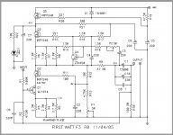
HI Thanks NO sorry i hadn't seen it, i will get on to it and get back to you.Confirm your pcb has all these components.
Record any differences to this circuit.
Circle which resistors are smoking on circuit.
Circle any other components you are concerned about.
- Status
- Not open for further replies.
- Home
- Amplifiers
- Pass Labs
- Nelson Pass F3 amplifier help wanted