Hello everybody
I need your help in the design of the amplifier
In pdf page 17
is the schematic of the amplifier
http://www.linearsystems.com/lsdata/files/Denis Vilfort Burning Amp Slides 2019.pdf
My questions :
- Is it possible to build it with a lower supply voltage (2 * 28V)?
- with 2SK1058 / 2SJ162 transistors Renaissance?
- with transistors of the BC550 / BC560 series in LTP (or their SMD equivalents)
I tried to do simulations in LTSpice but I'm not an engineer so I don't have the proper knowledge (only by trial / error method ;-)
Thank you
Document lacks page numbers, can you be explicit about which amp you are talking about please, the Hitachi or the symmetric?
These amps lack constant current sources in places so will need various resistor values adjusting if the supply voltage is changed to maintain the same bias currents. Lower supply voltage will just lower the output power and is OK, but note that you need a fair few volts headroom with lateral MOSFETs - they need this to drive the gates, so +/-28V may mean clipping at 23V or so.
The 2SK1058/2SJ162 pair are also laterals so will work - as will Exicons
That symmetric circuit lacks gate-protection zeners, but if you substitute 2SK1058/2SJ162 that will fix that. Not sure why it has source-resistors, other than to allow easy measuring of bias current. Laterals don't need thermal compensation so these resistors only add to cross-over distortion slightly IIRC.
Laterals have source as the substrate connection, so omitting source resistors allows the output pair to avoid using heatsink pads if you isolate the heatsink electrically - the heatsink will ride at the output voltage then, or you can use a heat transfer block thats directly in contact with FETs but isolated from heatsink proper using a larger area pad for better thermal performance. Basically there are some extra options with the sources being substrate and commoned.
Laterals have source as the substrate connection, so omitting source resistors allows the output pair to avoid using heatsink pads if you isolate the heatsink electrically - the heatsink will ride at the output voltage then, or you can use a heat transfer block thats directly in contact with FETs but isolated from heatsink proper using a larger area pad for better thermal performance. Basically there are some extra options with the sources being substrate and commoned.
Whilst it works after a fashion once M2 is fixed its also pretty grim with regards to DC precision (high offset in standard form) and it also seems to have 100ma or so flowing in the VAS stage which gives an Iq somewhere in the 30kW (dissipation in each device) region... but LT doesn't care 🙂
Attachments
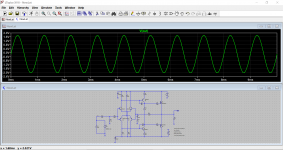
I tried your values (only in LTspice). It is good for low level signal, but for 1V input we have clipping at 9V for upper sine wave for 27V power supply
1V input for 45C power supply = clipping about 20V upper sine wave
Distortion about 0.7% is not impressive
Is there any sense to further improve this VSA circuit
I built a VSSA amp (really good amp) known in the forum but I would like to compare it with a different concept
1V input for 45C power supply = clipping about 20V upper sine wave
Distortion about 0.7% is not impressive
Is there any sense to further improve this VSA circuit
I built a VSSA amp (really good amp) known in the forum but I would like to compare it with a different concept
if you want an amp that works really well and based on k1058 and j162, I recommend this one.
I assembled it almost 15 years ago and I still love it as much.
I can find you the complete file (in French) for the assembly, the settings and what to do the pcb).
it is simple, efficient, always happy and musical
http://jm.plantefeve.pagesperso-orange.fr/30W_nrds.gif
I assembled it almost 15 years ago and I still love it as much.
I can find you the complete file (in French) for the assembly, the settings and what to do the pcb).
it is simple, efficient, always happy and musical
http://jm.plantefeve.pagesperso-orange.fr/30W_nrds.gif
celui là aussi ,assemblé il y a plus de 10 ans .
plus dure a mettre au point ,mais quel bonheur !!
il faut juste jouer un peu avec la contre reaction
http://jm.plantefeve.pagesperso-orange.fr/zenotron.gif
http://jm.plantefeve.pagesperso-orange.fr/zenotron_module.jpg
plus dure a mettre au point ,mais quel bonheur !!
il faut juste jouer un peu avec la contre reaction
http://jm.plantefeve.pagesperso-orange.fr/zenotron.gif
http://jm.plantefeve.pagesperso-orange.fr/zenotron_module.jpg
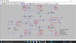
VSA mods
Looks doable. Check out the attached mods.
Zeners for current limiting SOA
Zeners for regulated tail current and less ripple.
Diodes for idle current so it is not so dependent on VAS current variations with ambient temp. These diodes should not on the heatsink since laterals have negative temp-co with >50mA bias. If you laterals have higher threshold voltage than the models just change the Schottky for 1N4148. If still more needed use 2x1n4148 plus Schottky.
100nF across rails close to lateral drains is very useful for stability.
Different gate resistors helps to balance the p- and n- rolloffs.
Compensation adjusted for no peaking using AC sweep. An actual amp may need a bit extra due to parasitics.
BC550/560 can be used to maybe 45V rails but the output stage will need parallel pairs or one 20x20 Exicon dual-die pair.
All the best.
Hi ZoltanChivay,...Is there any sense to further improve this VSA circuit
Looks doable. Check out the attached mods.
Zeners for current limiting SOA
Zeners for regulated tail current and less ripple.
Diodes for idle current so it is not so dependent on VAS current variations with ambient temp. These diodes should not on the heatsink since laterals have negative temp-co with >50mA bias. If you laterals have higher threshold voltage than the models just change the Schottky for 1N4148. If still more needed use 2x1n4148 plus Schottky.
100nF across rails close to lateral drains is very useful for stability.
Different gate resistors helps to balance the p- and n- rolloffs.
Compensation adjusted for no peaking using AC sweep. An actual amp may need a bit extra due to parasitics.
BC550/560 can be used to maybe 45V rails but the output stage will need parallel pairs or one 20x20 Exicon dual-die pair.
All the best.
Attachments
Last edited:
Hi
I thing about symmetric
here is sim file
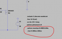
p-channel device is backwards.
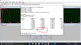
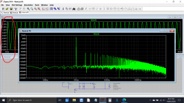
Use a short time slice to get accurate distortion measurements on the FFT.
BC550/560 can be used to maybe 45V rails but the output stage will need parallel pairs or one 20x20 Exicon dual-die pair.
I'd disagree, 45V and single output pair will drive 8 ohms, although doubling up will give better voltage headroom and less stress. No secondary breakdown makes lat fets tough as old boots like this! I built a +/-47V amp in the 1980's and its still running nicely (re-capped at some point, original Hitachi MOSFETs still).
I tried your values (only in LTspice). It is good for low level signal, but for 1V input we have clipping at 9V for upper sine wave for 27V power supply
1V input for 45C power supply = clipping about 20V upper sine wave
Distortion about 0.7% is not impressive
Is there any sense to further improve this VSA circuit
I built a VSSA amp (really good amp) known in the forum but I would like to compare it with a different concept
This is at the point of clipping (20 volts peak) and also at '1W/8ohm'.
Use your own models and tweak the bias set resistor R15 to give around 100ma current in the FET's. Make sure you set the timestep correctly for the distortion tests and run the sim long enough to get a good result.
Attachments
Thank you very much for your help
I think I'll start building a prototype
I will inform you about any progress
I think I'll start building a prototype
I will inform you about any progress
- Home
- Amplifiers
- Solid State
- Neeed help with Lateral Mosfet amp