Oh, understood, Chris. Previously, as soon as the delay relay engaged upon turn-on, there was DC on the output of the right channel that decreased only a few mA as the unit stabilized.
Thank you again,
Greg
Thank you again,
Greg
Audire Andante Test Results
I've finally gotten back to work on the Andante, and have taken measurements of the matched dual transistors as well as the rail voltages and DC offset for each channel - spreadsheet is attached.
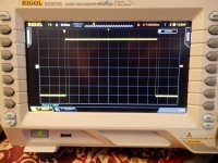
I've also added some 'scope pictures of each channel with a sine wave at the input, and with the volume turned up. DC-coupled as advised. Looks good, but the DC offset is huge on the right channel, as measured with my Fluke. I did use the 'scope to look at rough voltages on the matched dual transistors as Chris suggested, but ended up using the Fluke 287 for more accurate readings, and it didn't seem like the meter changed readings at all.
Note that the offset is low with the tone circuit bypassed, and shoots way up with the tone circuit engaged. These readings come up as soon as the unit turns on; there is no other fault event that makes this happen.
I am pretty sure now that the upper section in the photos is the line amplification stage, and the lower section is the tone stage, based on following traces. Readings on the Qs don't change with the status of the tone defeat switch. The only thing I see different from Left to Right channel is the readings on Q1 in the line stage of the Right channel; they are about 0.2V lower than those on the Left.
What other measurements should I take to help figure this out?
Thank you!
I've finally gotten back to work on the Andante, and have taken measurements of the matched dual transistors as well as the rail voltages and DC offset for each channel - spreadsheet is attached.
I've also added some 'scope pictures of each channel with a sine wave at the input, and with the volume turned up. DC-coupled as advised. Looks good, but the DC offset is huge on the right channel, as measured with my Fluke. I did use the 'scope to look at rough voltages on the matched dual transistors as Chris suggested, but ended up using the Fluke 287 for more accurate readings, and it didn't seem like the meter changed readings at all.
Note that the offset is low with the tone circuit bypassed, and shoots way up with the tone circuit engaged. These readings come up as soon as the unit turns on; there is no other fault event that makes this happen.
I am pretty sure now that the upper section in the photos is the line amplification stage, and the lower section is the tone stage, based on following traces. Readings on the Qs don't change with the status of the tone defeat switch. The only thing I see different from Left to Right channel is the readings on Q1 in the line stage of the Right channel; they are about 0.2V lower than those on the Left.
What other measurements should I take to help figure this out?
Thank you!
Attachments


Last edited:
Hi Greg,
It's clear from the DC offset readings that your right channel diff pair isn't well matched. The figures are about the only thing we can say anything about because your measurements on the fets themselves don't have any context (we need a schematic for that). You pretty much haveto ignore those unless you reference all the readings to the source. Readings to the ground do not really mean anything until we know how they relate (need a schematic for that).
The fact that DC offsets change a lot when the tone section is switched in is very suspicious. The action of the bass control is hinted at only. What we need are measurements with the bass control at neutral for tone in and out, then another reading with the bass control at maximum and minimum.
Sometimes I like to see what he differential is between the two gates, but with JFets, this is an extremely high impedance node (well, it can be) and it may not take kindly to a meter hung across the two points. Measuring each to ground isn't helpful if the circuit is working since the offset between them should be small. You can think of a differential pair as an Op Amp with low gain. A linear circuit will do whatever it takes within reason to maintain the + and - phase inputs (the two gates) at equal potentials. If they are not well matched, there will be an offset voltage present that is higher with the degree of mismatch. This will also show up on the output as a DC offset. Light bulb might come on right about now if you're sharp. Let's say there is a 5 mV DC voltage on the non-inverting input. The other gate is tied to the output through a resistor, and another to ground (often a capacitor blocks DC current). So if the negative phase input is sitting at 10 mV offset, the feedback action will cause the output to be set at a voltage that through the feedback network causes the negative phase to also be 5 mV. Note that I used positive values or there would have been a (-) in front of the value. So the negative phase will track the voltage on the positive phase input unless it can't due to component failure or it runs out of supply voltage (clipping).
So if the feedback is 20 dB (X0.1), in order to make an equal change in voltage on the negative phase, the output has to be 10 X higher than the input side (positive phase). The voltage at the output is attenuated by a factor of 10 before it gets to the negative phase side (feedback side).
I probably didn't explain it as clearly as when I'm fully awake, but hopefully you got the idea. Now, at DC, if there is a capacitor blocking DC current flow to ground in the feedback network, the gain at DC falls to be unity, one. So including a capacitor will reduce DC offsets by a factor equal to the AC gain of the circuit. That's why you will often see a capacitor in the ground side of the feedback network. You can even go further and use an Op Amp as a "DC servo" to achieve very low DC offsets.
So all of the above assumes a matched pair. What if they aren't matched? Then the diff pair balances with a DC offset which will be seen in the output voltage. This is what I can see in your amplifier just by your voltage readings. I don't like the 48.6 mV reading as my maximum limit is 50 mV. Anything above 50 mV is completely unacceptable from my point of view. But, I have seen amplifiers designed with a DC offset of 250 mV using a well matched pair (you can figure out the expected offset from the schematic and device parameters. We used to use a calculator, but today most people might simulate it instead. But for this ... you guessed it, you need a schematic. Many good amplifier designers design for a 0 mV DC offset and the reality of parts means that most will be below 30 mV. But then it is a question of the matching in the diff pair (your transistor matched pairs in the single can).
Let me know if I confused you or not.
-Chris
The figures are about the only thing we can say anything about because your measurements on the fets themselves don't have any context (we need a schematic for that). Readings to the ground do not really mean anything until we know how they relate (need a schematic for that).
OK, I took those because earlier you wanted to see gate-source voltages, but I understand about the lack of context, for sure. I really do wish I could come up with a schematic, but I think the chances are slim to none.
The fact that DC offsets change a lot when the tone section is switched in is very suspicious. The action of the bass control is hinted at only. What we need are measurements with the bass control at neutral for tone in and out, then another reading with the bass control at maximum and minimum.
OK, I'll take a measurement with bass control at neutral with tone in. I already confirmed it makes no difference with tone out (defeated). What I noticed before is it rises from the minimum shown in the table to the maximum as I adjust the control, so neutral setting will likely be around the middle of the max DC offset shown, or about 400mV for the right channel.
Sometimes I like to see what he differential is between the two gates, but with JFets, this is an extremely high impedance node (well, it can be) and it may not take kindly to a meter hung across the two points. Measuring each to ground isn't helpful if the circuit is working since the offset between them should be small. You can think of a differential pair as an Op Amp with low gain. A linear circuit will do whatever it takes within reason to maintain the + and - phase inputs (the two gates) at equal potentials. If they are not well matched, there will be an offset voltage present that is higher with the degree of mismatch. This will also show up on the output as a DC offset. Light bulb might come on right about now if you're sharp.
I'm sharp, but not so much about this master class stuff.
Let's say there is a 5 mV DC voltage on the non-inverting input. The other gate is tied to the output through a resistor, and another to ground (often a capacitor blocks DC current). So if the negative phase input is sitting at 10 mV offset, the feedback action will cause the output to be set at a voltage that through the feedback network causes the negative phase to also be 5 mV. Note that I used positive values or there would have been a (-) in front of the value. So the negative phase will track the voltage on the positive phase input unless it can't due to component failure or it runs out of supply voltage (clipping).
Are you referring in the above to what is occurring within the matched duals?
So if the feedback is 20 dB (X0.1), in order to make an equal change in voltage on the negative phase, the output has to be 10 X higher than the input side (positive phase). The voltage at the output is attenuated by a factor of 10 before it gets to the negative phase side (feedback side).
Again, are you describing the feedback action occurring within the two sides of this dual transistor? I'm guessing you are not referring to negative feedback being applied from the output of this preamp to the pairs, right? Or am I incorrect, and the preamp utilized feedback for correction?
I probably didn't explain it as clearly as when I'm fully awake, but hopefully you got the idea. Now, at DC, if there is a capacitor blocking DC current flow to ground in the feedback network, the gain at DC falls to be unity, one. So including a capacitor will reduce DC offsets by a factor equal to the AC gain of the circuit. That's why you will often see a capacitor in the ground side of the feedback network. You can even go further and use an Op Amp as a "DC servo" to achieve very low DC offsets.
Of course, I've seen this plenty of times in amps, but didn't realize it was used in preamps.
So all of the above assumes a matched pair. What if they aren't matched? Then the diff pair balances with a DC offset which will be seen in the output voltage. This is what I can see in your amplifier just by your voltage readings. I don't like the 48.6 mV reading as my maximum limit is 50 mV. Anything above 50 mV is completely unacceptable from my point of view.
Gotcha. Having almost 1V of offset in this preamp is really scary. Now I know why it burned up my brother's amplifier.
But, I have seen amplifiers designed with a DC offset of 250 mV using a well matched pair (you can figure out the expected offset from the schematic and device parameters. We used to use a calculator, but today most people might simulate it instead. But for this ... you guessed it, you need a schematic. Many good amplifier designers design for a 0 mV DC offset and the reality of parts means that most will be below 30 mV. But then it is a question of the matching in the diff pair (your transistor matched pairs in the single can).
Just to be clear, we are talking about a preamplifier, not an amplifier, but we're really talking the same principals, right?
Unfortunately, the message seems to be that there isn't really a way to resolve this without a schematic (tell me I'm wrong, please).
Let me know if I confused you or not.
Hahaha. Me, confused?

Thanks very much for your time, Chris,
Greg
One more observation, Chris. The left channel DC offset with the tone controls engaged and the bass on full is also really high - 240mV. Does that suggest a problem with the matched dual for the tone control in that channel as well?
Cheers,
Greg
Cheers,
Greg
Hi Greg,
Okay, past my bedtime but let's see if I can make any sense.
I was thinking power amplifier, but it doesn't matter as a preamplifier is the same thing with (usually) less voltage swing and much lower current sourcing ability. With a preamplifier there is a much higher emphasis on low noise circuitry. See, I'm pretty tired!
Try to measure between the two gates The voltage reading should be very, very small. I'm glad you bought a Fluke right about now!
I'm considering a working gain circuit where you will have the diff pair, and the rest of the circuitry to make up that gain block. This block you can see called things like "flat amp", "EQ Amp", "Tone amplifier" and things like that. The most basic thing that differs between them is what is in their feedback network. Other than that they could be the same circuit. So a complete circuit with the diff pair, Vas (Voltage amplification stage) and perhaps a current buffer so it can drive cables or even the feedback network. A very little power amplifier. Sorry I wasn't that clear before.
One change though. With preamplifiers, I don't want to see even 5 mV on the output. Coupling capacitors should be used where possible. Special low impedance outputs, like true balanced lines, can't use coupling capacitors without degrading the signal if you actually do drive a 600R load.
-Chris
Okay, past my bedtime but let's see if I can make any sense.
I was thinking power amplifier, but it doesn't matter as a preamplifier is the same thing with (usually) less voltage swing and much lower current sourcing ability. With a preamplifier there is a much higher emphasis on low noise circuitry. See, I'm pretty tired!
Try to measure between the two gates The voltage reading should be very, very small. I'm glad you bought a Fluke right about now!
Again, are you describing the feedback action occurring within the two sides of this dual transistor? I'm guessing you are not referring to negative feedback being applied from the output of this preamp to the pairs, right? Or am I incorrect, and the preamp utilized feedback for correction?[/QUOTE]Are you referring in the above to what is occurring within the matched duals?
I'm considering a working gain circuit where you will have the diff pair, and the rest of the circuitry to make up that gain block. This block you can see called things like "flat amp", "EQ Amp", "Tone amplifier" and things like that. The most basic thing that differs between them is what is in their feedback network. Other than that they could be the same circuit. So a complete circuit with the diff pair, Vas (Voltage amplification stage) and perhaps a current buffer so it can drive cables or even the feedback network. A very little power amplifier. Sorry I wasn't that clear before.
Yes, it isn't that uncommon in discrete circuits, sometimes with Op Amps too.Of course, I've seen this plenty of times in amps, but didn't realize it was used in preamps.
I've seen that kind of output voltage on other preamplifiers, and the amps from the same manufacturer did not use a blocking capacitor on the input either. Same thing happened. Burned woofer, amplifier survived. Woofer wasn't cheap, more than an amplifier repair.Gotcha. Having almost 1V of offset in this preamp is really scary. Now I know why it burned up my brother's amplifier.
Well, actually we just have to think in terms of circuit blocks and what they usually do.Unfortunately, the message seems to be that there isn't really a way to resolve this without a schematic (tell me I'm wrong, please).
One change though. With preamplifiers, I don't want to see even 5 mV on the output. Coupling capacitors should be used where possible. Special low impedance outputs, like true balanced lines, can't use coupling capacitors without degrading the signal if you actually do drive a 600R load.
-Chris
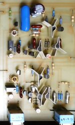
As seen from your pictures this is a dual mono preamp with completely independent
channels in mirror image board fashion.
Both tone and line stage are set up as discrete operational amplifiers with dual
n-channel j-fet input, the differential stage having a current regulator diode in the
common source line and current mirrors as drain loads. The rest of the circuit may
be similar to what you know from j-fet input style power amps and j-fet integrated
op-amp internal circuitry. In other words we have to deal with four "channel diff pair"s
here not only one in the right channel as suggested before.
Tone stage and line stage have a similar layout, but on the tone stage the 470μF 16V
electrolytic cap responsible for unity gain at dc is missing. I am not sure why. This may
be due to the feedback mode of the tone controls and is an explanation why offset rises
with bass full on. With a cap in the same position here the bass control operation may
be impaired.
From your screen pictures and your voltage readings it is obvious that the amp is not
defective - although (some of the) Vgs voltages are suspicious and look too high.
I suggest checking the 470μF caps for leakage now.
If this does not help I suggest a careful realignment. The trimmers are in fact for offset
zero. If you are sure that the two caps are fine try a sensible adjustment here, for each
of the four amp stages and checking their respective outputs for dc in millivolts range.
No wild rotation allowed here.
Yes, I said before do not touch the trimmers, but now I had a look at the board layout.
Your pictures however are not sufficient in resolution, viewing angle etc. to completely
see the schematic without drawing it.
I addition square wave pictures for about 1 kHz should be taken and please adjust the
time base of your scope in a way that only one or two wave lengths are shown, it is
useless and repetitive otherwise. This is easily done at a generator frequency of 1.1 kHz.
Hi as_audio,
I didn't know about the coupling capacitor. With that knowledge I believe you have probably found the most likely source of trouble. However, do not even talk about adjusting anything yet. Right now the main issues need to be solved. If there is a coupling capacitor on the input tot he main gain stage (amplifier stage), those would probably be a good idea to replace now as well.
Why we shouldn't adjust anything yet? The preamp worked fine with those adjustments. So we are talking about a component failure. I suspect that if the diff pairs need to be replaced, then you might need to make adjustments, but not before.
-Chris
To clarify, I had not suggested there was only one diff pair to be concerned about. I wanted to focus on the main pair, then get to the tone control stage after the main stage was looked after. One thing at a time so that we don't develop confusion - agreed?In other words we have to deal with four "channel diff pair"s
here not only one in the right channel as suggested before.
I didn't know about the coupling capacitor. With that knowledge I believe you have probably found the most likely source of trouble. However, do not even talk about adjusting anything yet. Right now the main issues need to be solved. If there is a coupling capacitor on the input tot he main gain stage (amplifier stage), those would probably be a good idea to replace now as well.
Why we shouldn't adjust anything yet? The preamp worked fine with those adjustments. So we are talking about a component failure. I suspect that if the diff pairs need to be replaced, then you might need to make adjustments, but not before.
-Chris
I suggest to take care of the dc offset first.
I did not write about a coupling cap in the usual sense but one connected like this:
see attached picture (note that I will not take responsibility for assumptions this
schematic being generally applicable to the Audire preamp).
The four "building blocks" are dc coupled.
We have no component failure here (except maybe for said elcaps). Have a look
at the board and the measurements and you will probably agree.
My proposals in post 27 are still valid and the sequence is clear.
Attachments

Last edited:
Hi as_audio,
-Chris
Absolutely agree ...I suggest to take care of the dc offset first.
Perfect, thank you. That is exactly what I was describing verbally.I did not write about a coupling cap in the usual sense but one connected like this:
Yes, exactly and I fully agree. I just fixed a preamp that had an almost 100% failure rate on the tantalum capacitors (gone leaky, not shorted). That unit was made in the mid-70's.We have no component failure here (except maybe for said elcaps).
-Chris
Final remark, the offset is positive, but the negative pole of this elcap is connected to the amp inv input.
This may lead to a very small leakage current which should disappear after adjustment.
A bipolar (non polarised, NP) electrolytic cap is usually preferred in a position like this and is easily available even on E*y.
This may lead to a very small leakage current which should disappear after adjustment.
A bipolar (non polarised, NP) electrolytic cap is usually preferred in a position like this and is easily available even on E*y.
Thank you both, very much, for your discussion and help with the preamp. I am heading out to for the day, and won't get back to the Andante until this evening.
However, for some relevant info:
All of the electrolytics are brand new - they were the first thing I replaced when I found a couple leaking in the power supply section.
No other caps have been removed from the unit - Julius was the last to work on this, and there is no location where a part is not present. The previous repairs were apparently to the power supply section, and I think, an added polystyrene bypass cap in the line amp section.
I'll do the square wave test. I have many other photos, if you think they would help with understanding the layout/schematic. I can also backlight the board again and take better pics that show the components as well as traces.
Chris - you mentioned measuring between the two gates; are you saying to use the meter with probes on both gates?
Thank you both, Chris and as-audio! I'll get back to you soon.
Cheers,
Greg
Hi Greg,
Yes. Let's se what measurement you get. If you can set that meter to a mV range and high impedance, do that please.
-Chris
Yes. Let's se what measurement you get. If you can set that meter to a mV range and high impedance, do that please.
-Chris
Hello Gentlemen,
Working back from the last recommendation from Chris, here are the gate to gate readings:
Left Channel
Line matched dual - 11mV
Tone matched dual - 6mV
Right Channel
Line matched dual - 45mV
Tone matched dual - 18mV
Next I'll put a square wave through as as_audio instructed.
Thank you both,
Greg
Working back from the last recommendation from Chris, here are the gate to gate readings:
Left Channel
Line matched dual - 11mV
Tone matched dual - 6mV
Right Channel
Line matched dual - 45mV
Tone matched dual - 18mV
Next I'll put a square wave through as as_audio instructed.
Thank you both,
Greg
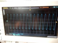
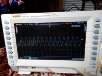
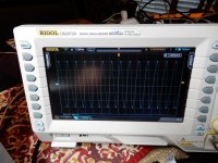
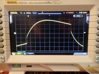
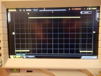
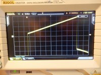
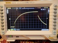
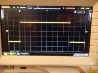
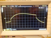
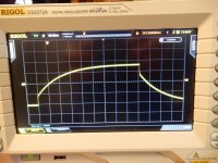
Wave forms each channel
OK, here are the wave forms. Left channel are in this post, right channel will follow. They may have uploaded out of order. The captions indicate position of tone defeat switch (Tone_Off), and Bass and Treble positions (e.g. B_Full_T_Half).
Volume on the preamplifier was a little higher for the left channel readings, but were reduced for the right channel readings to show the entire wave form for full bass and treble, which I also adjusted for the left channel.
They look pretty much identical to me. The effect of the tone controls appears fairly substantial, which was how they sounded for the brief period I could operate the preamp before it caused my amps to shut down.
Are there any other readings I should take next, Obi Wan(s)?
Attachments

Last edited:
Right channel.
Images are not in correct order, but hovering the pointer over the thumbnail shows the file name, so right and left channel pics can be compared.
Thank you,
Greg
Images are not in correct order, but hovering the pointer over the thumbnail shows the file name, so right and left channel pics can be compared.
Thank you,
Greg
Attachments
Last edited:
Hi Greg,
Yes, that pretty much confirms what I was thinking just by looking at your DC offset figures.The right channel diff pairs need replacing. The left channel might be better with the 6 mV pair in the main amplifier, but that's being real picky. Something you can try after the rest is working properly.
-Chris
I am very grateful for the input you are both providing, and respect what each of you is indicating. Thank you for taking your time to help me with this.
It seems that although there may be a risk in starting with the adjustments that as_audio has recommended, it seems like it might be a reasonable incremental approach if I carefully document starting voltages and effects after adjusting. It might also satisfy a couple of goals. First, to learn about the circuit interactions as I make the minimal adjustsments, and second, to eliminate the potential of faulty matched dual transistors. The results will hopefully validate one position or the other. I will then be more prepared for replacing them as Chris has suggested if the adjustments don't work.
Does this sound reasonable?
As_audio; I am not sure I follow what you are proposing I do in your post #31. Is this a suggestion to add a polarized cap to the preamp, or replace the polarized 470uF with a non-polarized? The caps at the line amp portion of the circuit are brand new Nichicon replacements, and the unit had this problem before any cap replacement. As an added precaution, I'll pull them and test with my LCR meter and my Fluke DMM.
Thank you both very much. Sorry to be so far below your knowledge levels, but I am very much enjoying the opportunity to learn that you are both providing.
Best to you both,
Greg
Hi as_audio,
It's okay that you don't agree, but not okay without a valid reason. Comments? After all, solving a problem at the source is always the best solution and I do have a fair amount of experience here.
If you have a good and valid reason I will certainly reconsider my suggestion.
Best, Chris
It's okay that you don't agree, but not okay without a valid reason. Comments? After all, solving a problem at the source is always the best solution and I do have a fair amount of experience here.
If you have a good and valid reason I will certainly reconsider my suggestion.
Best, Chris
- Home
- Source & Line
- Analog Line Level
- Need Your Assistance - Audire Andante