Hi,
I’m planning to build a dac and I’m getting a bit lost in clock division for reclocking. I will be using a cs8412 in mode 3 (fs and bck are inputs), I2S separator as per the design by Pedja Rogic to tda1541’s in balanced mode.
I intend to use a 11,289 clock which I will divide down to 2,83 mhz for bck and 44,1 khz for fs. Previously I’ve used a 4040 counter for division as it is used in the dddac but I know this might not be the best solution. Another option is using cascaded 74hc74’s like used by mr Tent. But while reading up I came across synchronous and asynchronous binary counter circuits that might also work. Would it be advisable to use such a synchronous counter circuit (example: [URL="http://www.electronics-tutorials.ws/counter/count_3.html) or does it make more sense to use cascaded 74hc74’s?
I’m looking for a compromise between simplicity and the best solution because I will have to design the pcb myself and I want to keep the complexity within reasonable limits. So if I can limit the design to 3 to 4 logic chips I’d like that.
Regards,
Joris
Btw I am planning for a clock output to slave the transport to the dac clock.
edit:link
Last edited:
Hi,
Thanks, I'll read up some more but that's what my feeling is as well. Now to find a decent way to layout the pcb...
regards
Joris
Thanks, I'll read up some more but that's what my feeling is as well. Now to find a decent way to layout the pcb...
regards
Joris
I’m planning to build a dac and I’m getting a bit lost in clock division for reclocking. I will be using a cs8412 in mode 3 (fs and bck are inputs), I2S separator as per the design by Pedja Rogic to tda1541’s in balanced mode.
This setup will lead to repeated / dropped samples. This will be audible as periodic clicks. These clicks are easiest to hear with sine wave test tones, the larger the frequency difference the shorter the time between the clicks.
The clicks are caused by the fact that the PLL clock inside the CS8412 is still used to decode incoming SPDIF signal (clock #1) and the external clock (clock #2) determines the moment this data is clocked out. Since both clocks don't run in sync and it is likely frequencies differ / drift up to 200ppm, samples have to be dropped / repeated, this causes the clicks.
Only way to get rid of the clicks is perfectly synchronizing both clocks using a (D)PLL or frequency tracker circuit based on a microcontroller for example.
The dividers need to be synchronous dividers like the 74xx161 series. The 74xx4040 series are non-synchronous ripple counters that add significant jitter (typical 200ps on BCK). With synchronous counters there is a fixed propagation delay between clock and each output as all outputs change simultaneously (synchronous). The outputs of a ripple counter change sequentially (compare it with domino effect), so the last output will have largest propagation delay (and jitter). For 11.2896 MHz clock this will lead to approx. 200ps of jitter added to the BCK signal and approx. 800ps added to the WS signal.
The PLL clock from the CS8412 usually has slightly lower jitter compared to the derived BCK and WS signals. So I suggest to run CS8412 in master mode instead, using MCK signal to synchronously reclock BCK, DATA, and WS signals.
All I2S signals need to have lowest possible jitter, if only WS and BCK are reclocked, jitter still passes through DATA signal (crosstalk).
In order to minimize jitter in the synchronous reclockers (D-flip-flops), use D flip-flops with shortest propagation delay (CLK > Q). The HC(T) series will work, but will add approx. 100ps of extra jitter for each flip-flop and approx. 50ps of extra jitter for each (cascaded) gate.
Best is to integrate DAC with source (when possible), skip the flawed SPDIF interface and use direct I2S between source and DAC. Then use a common low jitter clock to drive both source and DAC.
The best external DAC applications require slaving the source through a clock signal that's fed back from DAC to source, or a servo system that will synchronize both source and DAC clock. Here it is also advised to use I2S interface instead of SPDIF like with the Zanden Transport / DAC. Typical jitter with highly optimized slaved source will be approx. 50ps.
What Slaving Does : LessLoss high end audio power cables, audiophile power cables, audiophile cables
Last edited:
Hi Ecdesigns,
Thanks for your reply. I still have to read it a couple of times before i fully understand. I'll do some further reading as well.
Unfortunately combining the transport and dac in to one is not an option due to the chosen case format. There simply is not enough space. I do plan on having a clock output for slaving the transport (like the tentlink). That should solve the repeated/dropped samples issue I thought (?) because all clocks should then run in sync.
As i want the option to use the dac with other transports as well I'd like to keep the spdif interface (flawed as it is) but i will think about direct i2s. Maybe using a pin header in the i2s lines is an option so i can use spdif via jumpers and i2s through an add on board. I'll think about it.
As far as I understand your post now I think you say that a synchronous clock divider is to be preferred. I think I saw such a circuit by you for dem clocking (74xx161?). I haven't drawn that out in to a logic schematic yet.
The link I tried to post gives two examples of such a synchronous divider on page 3. Is that something I should examine further and compare to the dem clock schematic mentioned above? At first glance the master clock is always in control and reclocks each division.
I will think about including a switching option between using the cs8412 in master mode and mode 3 (dip switch for mode selection and pin header+jumper in the I2s lines). I'm also considering a combination: divide by 4 using 74xx74's as per mr Tents schematic for bck and then a synchrounous divider for ws.
Please note that even though I've build a few dac's, this is the first time i'm actually trying to make my own choices in the design. Sort of experimental cooking instead of following the recipe and without any proper training or education. So if I say a few dumb things, tell me but don't send the inquisition after me please.
One more question. You refer to reclocking sdata. I thought that when using mode 3 Sdata would be reclocked in the cs8412 buffer? And even without all the previous I'm going to separate i2s in to separate left and right datastreams. If reclocking sdata is that important would it be wise to reclock sdata (and bck ws) after the i2s splitter? And if so should i do it before the i2s splitter as well?
Thanks again for your response and Poynton's. In the end the choiches i make will depend both on circuit/performance considerations and my ability to design the pcb layout. This is way complex and very difficult to me.
Kind regards,
Joris
hi jazz,
I'm interesting how are you succesfull in your project?
I'm also doing something like you except I want to "feed" Pedja Rogic's I2S splitter from different sources: SPDI_1-DIR9001, SPDIF_2-CS8414, direct I2S from CD player and from Valab's Teralink USB to I2S receiver.
I'm going to make reclocking on MLCK basis AT LEAST after I2S splitting because HEF4517 and 74157 will add delay more than 200ns from front edge of BCK.
I gues also to try delay BCK for 1, 2 or 3 period of MLCK because period of BCK is about 354ns if you gonna use 64bit frame I2S.
On the other hand, recloking I2S after receiving it from transport also can be reasonable, except this will also add some jitter 🙄.
Best wishes
Saulius
I'm interesting how are you succesfull in your project?
I'm also doing something like you except I want to "feed" Pedja Rogic's I2S splitter from different sources: SPDI_1-DIR9001, SPDIF_2-CS8414, direct I2S from CD player and from Valab's Teralink USB to I2S receiver.
One more question. You refer to reclocking sdata. I thought that when using mode 3 Sdata would be reclocked in the cs8412 buffer? And even without all the previous I'm going to separate i2s in to separate left and right datastreams. If reclocking sdata is that important would it be wise to reclock sdata (and bck ws) after the i2s splitter? And if so should i do it before the i2s splitter as well?
Thanks again for your response and Poynton's. In the end the choiches i make will depend both on circuit/performance considerations and my ability to design the pcb layout. This is way complex and very difficult to me.
Kind regards,
Joris
I'm going to make reclocking on MLCK basis AT LEAST after I2S splitting because HEF4517 and 74157 will add delay more than 200ns from front edge of BCK.
I gues also to try delay BCK for 1, 2 or 3 period of MLCK because period of BCK is about 354ns if you gonna use 64bit frame I2S.
On the other hand, recloking I2S after receiving it from transport also can be reasonable, except this will also add some jitter 🙄.
Best wishes
Saulius
Hi Saulius,
Well i did find the 74hc590 which would allow me to keep clock division on one chip and keep it synchronous as well. Fit's the bill nicely.
Guess i'm lagging behind because I havn't given propagation delay much consideration yet (new to digital design, though i have build various dac's from others schematics). I'd have to compare the 74hc590 to the 161 to get an idea yet have little to no clue about it's real effect.
Still thinking about reclocking. I don't want to use 3 quad flipflop's for that so i'm gonna search for a single or dual dip style flipflop. I take your point about placing it after the i2s splitter. If i do it, i'll do it that way.
I'm curious about your reason for using two different recievers and the way you plan to do the switching between the various inputs. I've stalled that issue for now and will probably start with a pin header and some jumpers. If i decide to do the switching i'll probably do it later.
Because i've recently started a new job and just started on my first assignment i'm rather busy with a lot of travel time. Thus time is sparse and mostly spent on doing research and learning. The first concept design is expected in the fall in the most positive scenario. will probably do some breadboarding tests with the dac/iv stage (which is ready) first and do some testing of power supplies.
Kind regards,
Joris
You do not need to divide MCK this vale You have is for clock in at reckl.
But if You going to master mode on receiver chip You have to somehow to divide MCK make SCK and BCK. Mind the time delay of dividng lines and try to compensate this...
I am running the I2S splitter but not in balanced mode rather the L/L and R/R
working without any clicks with dual mono dac-s. I did not try the balanced splitter konfiguration.
with this rearranged circuit, which is predecessor of all same kind circuits
cheers
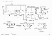
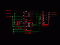
he scematic was published in
hi-fi news & record review, september 1990
part is balanced I2S splitter circuit
the chips are not marked but those are the same chips like in other similar cir.
HEF4517, 74HC157
Hi
here are attached few items:
1.the same picture published in 1990 HiFi News, but in better quality - easier to see number of input/outputs.
2. Second picture is same circuit but balanced I2S splitter part only.
3. the article of Pedja Rogic, where is mentioned this 1990 HiFi News schematic.
Please take into account 1990 HiFi News shematic is ok only for 32 bit word (all L and R bits transferred per 32 BCK, as after SAA7210 and SAA7310).
So, if you are going "to steal" I2S directly from CD player based of SAA7210 or SMD SAA7310, this is realy operational schematic.
For 64 bit word (most of SPDIF receivers) we need to use schematics proposed by Pedja.
Those two shematics should operate ok, but with 5V power suply for HEF4517 only for 44.1kHz sample rate. And mainly for NXP HEF4517, other clones of 4517 can be simply to slow.
For higher sample rates here is a way to increase power supply to 10 - 15V, almost proportionally decreasing propagation delay, but then you need to play with pull up resistors and diodes to protect 74HC157 inputs from overvoltage. The you can freely use not only NXP IC.
I'm going to use in my project both schematics as I have both types of I2S source - 32 and 64 bit frame.
Attachments

A 4040 is a ripple through counter.
Personally I would go for the synchronous counter for better accuracy.
Personally I would go for the synchronous counter for better accuracy.
64 bits word?
Maybe, but for booth channels😉
🙂 My mistake - word in I2S means only one channel, left or right.
As frame or subframe (as Pedja wrote in his article) I mean whole data frame needed for one stereo sample.
Hi,
Had some time and started thinking about the layout. That's progressing but while doing that I confronted myself with a question left open:
I intend to do clock locking between dac and transport. Yet i cannot find much information about the circuitry used for transporting the clock signal from the dac to the transport. Could somebody point me to a circuit for this? Or is it as simple as using a 74 hc04 buffer?
Kind regards,
Joris
I intend to do clock locking between dac and transport. Yet i cannot find much information about the circuitry used for transporting the clock signal from the dac to the transport. Could somebody point me to a circuit for this? Or is it as simple as using a 74 hc04 buffer?
When using external DAC, it will be impossible to get required low jitter levels in both, source and DAC. In general this solution will provide reduced jitter levels compared to non-slaved digital audio sources, but jitter amplitude will still be at least 10 times too high for plain 44.1/16 NOS that requires 3ps or less on-chip jitter (D/A conversion stage).
With slaved transport you have a relatively low jitter clock in the DAC and relatively high jitter clock in the external digital audio source. Other problem is that the required clock or DC-servo interlink will introduce an unwanted (RF) ground loop. When adding capacitive, inductive, or optical isolation circuits, source jitter is further boosted (cumulated jitter).
Also make sure the source (CD transport) receives an alternative clock when external DAC clock fails. Without this back-up clock you risk a servo lock-out that could result in CD player / CD damage. So you need a circuit that detects valid external clock and switches between external and backup clock.
Source jitter travels on the SPDIF signals and pollute DAC electronics upon their arrival. So jitter now simply enters the DAC in an indirect way.
Even if the DAC clock has zero jitter, the interference produced by SPDIF signal and extracted I2S signals will pollute power supplies and affect surrounding circuits by EMI. Finally this will result in interference and crosstalk that in turn leads to increased jitter levels on the DAC chip (D/A conversion circuit).
This is why I arrived at the conclusion that the slaved digital audio source is best integrated with the DAC so both receive lowest possible jitter clock. This method is already used in most CD players for good reason.
When the integrated digital audio source is able to maintain low jitter levels, then its effect on DAC chip D/A stage jitter will remain minimal.
As for the clock coupling I would advise to use screened twisted pairs interlink terminated with 110 Ohms, using RS422 transceivers. Suitable isolation transformers / filters can be sourced from obsolete computer network cards.
The RS422 transceivers run on 5V DC, in / output signals are TTL compatible and line drivers / receivers have differential outputs and inputs. The differential inputs need to be terminated with 110 Ohm resistors.
Here are the datasheets for DS8921 RS422 transceivers:
DS8921 - Differential Line Drivers and Receiver Pair
These transceivers will add approx. 6ps jitter, so driver / receiver jitter contribution equals approx. 12ps.
- Status
- Not open for further replies.
- Home
- Source & Line
- Digital Line Level
- need some advise in clock dividing